background image

2  Warning

2.1. 

Prevention  of Electrostatic  Discharge (ESD) to  Electrostatically


Sensitive (ES) Devices

Some semiconductor (solid  state)  devices can  be damaged  easily  by static electricity.  Such  components commonly are called  Elec­

trostatically Sensitive (ES)  Devices.

Examples of typical  ES  devices are  1C  (integrated circuits) and  some field-effect transistors and 

semiconductor “chip” components.

The  following  techniques  should  be  used  to  help  reduce  the  incidence  of  component  damage  caused  by  electrostatic  discharge 

(ESD).

1.  Immediately before  handling  any semiconductor component or semiconductor-equipped  assembly,  drain  off any ESD  on your 

body  by touching  a  known  earth  ground.  Alternatively,  obtain  and wear a commercially available  discharging  ESD wrist strap, 

which  should  be  removed  for potential  shock reasons  prior to applying  power to the  unit under test.

2.  After removing  an  electrical  assembly equipped with  ES  devices,  place the  assembly on  a  conductive  surface  such  as alumi­

num foil,  to  prevent electrostatic charge  buildup or exposure  of the assembly.

3.  Use  only a  grounded-tip  soldering  iron to  solder or unsolder ES devices.

4.  Use  only  an  antistatic solder removal  device.  Some  solder removal  devices  not classified  as "antistatic  (ESD  protected)"  can 

generate  electrical  charge  sufficient to damage  ES devices.

5.  Do  not use freon-propelled  chemicals.  These can  generate electrical  charges  sufficient to  damage  ES devices.

6.  Do  not  remove  a  replacement  ES  device from  its  protective  package  until  immediately before you  are  ready to  install  it.  (Most 

replacement  ES devices are  packaged with  leads electrically shorted together by conductive foam,  aluminum foil or compara­

ble conductive  material).

7.  Immediately before  removing the  protective  material  from the  leads of a  replacement ES  device, touch the  protective  material 

to the chassis or circuit assembly into which the device will  be  installed.

CAUTION  :

Be  sure  no  power is applied to the chassis  or circuit,  and  observe all  other safety precautions.

8.  Minimize  bodily  motions  when  handling  unpackaged  replacement  ES  devices.  (Otherwise  harmless  motion  such  as  the 

brushing together of your clothes fabric or the lifting of your foot from a carpeted floor can  generate static electricity (ESD) suf­

ficient to damage an  ES  device).

4

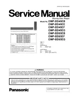
Содержание DMP-BD45EE

Страница 1: ...iced or repaired only by experienced professional technicians Any attempt to service or repair the product or products dealt with in this service information by anyone else could result in serious injury or death IMPORTANT SAFETY NOTICE There are special components used in this equipment which are important for safety These parts are marked by A in the Schematic Diagrams Circuit Board Diagrams Exp...

Страница 2: ...s Licenses 12 5 Location of Controls and Components 13 6 Operating Instructions 14 6 1 Taking out the Disc from BD Drive Unit when the Disc cannot be ejected by OPEN CLOSE button 14 6 2 Micro Fuse Conducting Check 15 7 Multiple Pressing Function 16 7 1 About the Multiple Pressing of the Unit s Remote Control 16 7 2 How to enter the Special Modes using the Multiple Pressing Function of the Unit s R...

Страница 3: ...to shock hazards 1 2 Leakage Current Cold Check 1 Unplug the AC cord and connect a jumper between the two prongs on the plug 2 Measure the resistance value with an ohmmeter between the jumpered AC plug and each exposed metal lic cabinet part on the equipment such as screwheads connectors control shafts etc When the exposed metal lic part has a return path to the chassis the reading should be betwe...

Страница 4: ...e of the assembly 3 Use only a grounded tip soldering iron to solder or unsolder ES devices 4 Use only an antistatic solder removal device Some solder removal devices not classified as antistatic ESD protected can generate electrical charge sufficient to damage ES devices 5 Do not use freon propelled chemicals These can generate electrical charges sufficient to damage ES devices 6 Do not remove a ...

Страница 5: ...be used until a replacement cover is obtained A replacement fuse cover can be purchased from your local Panasonic Dealer If the fitted moulded plug is unsuitable for the socket outlet in your home then the fuse should be removed and the plug cut off and disposed of safety There is a danger of severe electrical shock if the cut off plug is inserted into any 13 ampere socket If a new plug is to be f...

Страница 6: ...3 Precaution of Laser Diode CAUTION THIS PRODUCT UTILIZES A LASER USE OF CONTROLS OR ADJUSTMENTS OR PERFORMANCE OF PROCEDURES OTHER THAN THOSE SPECIFIED HEREIN MAY RESULT IN HAZARDOUS RADIATION EXPOSURE 6 ...

Страница 7: ... used The letter of PbF is printed either foil side or components side P b F on the P C B using the lead free solder See right figure Service caution for repair work using Lead Free Solder PbF The lead free solder has to be used when repairing the equipment for which the lead free solder is used Definition The letter of PbF is printed on the P C B usingthe lead freesolder To put lead free solder i...

Страница 8: ...ere the traverse unit optical pick up is placed and ground the sheet 2 6 2 Human body grounding Use the anti static wrist strap to discharge the static electricity from your body 2 6 3 When exchange the BDP Digital P C B Module Do not remove the FFC while replacing the BDP Digital P C B Modile Keep the BDP Drive and the Digital P C B connecting with it After repaired keep the BDP Digital Module co...

Страница 9: ... List for individual parts of BDP Digital P C B Module Exploded View and Parts List for individual parts of BDP Digital P C B Module 2 The following category are recycle module part Please send them to Central Repair Center BDP Digital P C B Module DMP BD45EB RFKNBD45EBT BDP Digital P C B Module DMP BD45EE RFKNBD45EET BDP Digital P C B Module DMP BD45EF RFKNBD45EFT BDP Digital P C B Module DMP BD4...

Страница 10: ... content using a registration code different from this unit s code you will not be able to play this content Authorisation Error is displayed Cancel the unit s registration Press to select Yes in DivX Registration Use the deregistration code to cancel the registration in www divx com Regarding DivX VOD content that can only be played a set number of times Some DivX VOD content can only be played a...

Страница 11: ...8 kHz sampling 4 Hz 44 kHz 96 kHz sampling 4 Hz 20 kHz 115 dB 100 dB 0 003 Optical terminal 1080p 1080i 720p 576p 480p TypeA 19 pin HDMI V 1 4 Content Type This unit supports HDAVI control 5 function BD Video BD RE BD R DVD Video DVD RAM DVD R DVD R DL DVD RW R RW R DL Music CD CD R CD RW SD card SD Memory Card from 8MB to 2GB SDHC Memory Card from 4GB to 32GB SDXC Memory Card 48GB 64GB USB device...

Страница 12: ...ation SDXC Logo is a trademark of SD 3C LLC DivX is a registered trademark of DivX Inc and is used under license Blu ray Disc is a trademark BD LIVE logo is a trademark of Blu ray Disc Association BONUSVIEW is a trademark of Blu ray Disc Association YouTube and Picasa are trademarks of Google Inc The Wi Fi CERTIFIED Logo is a certification mark of the Wi Fi Alliance DLNA the DLNA Logo and DLNA CER...

Страница 13: ...Displaying Title View and Album View screens Operating contents of VIERA CAST IBD65 Transmit the remote control signal OPEN CLOSE button CAUTION Do not place objects in front of the unit The disc tray may collide with objects when it is opened and this may cause injury Volume up down button Amplifier receiver AUDIO button RE MASTER button Select drive BD DVD CD SD card or USB device button IBD651 ...

Страница 14: ...layed on the unit s FL display 3 Press OK button on the remote control or OPEN CLOSE button on the unit 6 1 1 2 When the power can not be turned off Press POWER button on the unit for over 4 seconds to turn off the power forcibly and step 1 to 3above 6 1 2 When the Forcible Disc Eject can not be done 1 Turn off the power and pull out AC cord 2 Remove the Top Case 3 Put the unit so that bottom can ...

Страница 15: ...6 2 Micro Fuse Conducting Check This unit uses the Micro Fuse Check the Micro Fuse conducting using the Tester at the check points below 15 RI006 D06F68SJA030 ...

Страница 16: ...tial settings and the Service Mode etc The Multiple Pressing function is not available for conventional models remote control Use the remote control included this unit 7 2 How to enter the Special Modes using the Multiple Pressing Function of the Unit s Remote Control For pressing the multiple buttons of the remote control this unit can be entering each of the following special modes After enterin...

Страница 17: ... Press and Hold Initialization of the Progressive Setting Initialize the Progressive setting and switch the display mode to the Interlace mode When pressing and holding the Stop button remote control main unit instead of the OK button current menu is moved to 10 OCL Disc Tray Lock Unlock setting ON Yes No 05 P N n OK Press and Hold Switch the TV System Switch the TV system to another one If the cu...

Страница 18: ...D Video 7 2 3 Privately Mode 2 Remote Cont Buttons 5 9 Red When pressing the 3 buttons 5 9 and Red simultaneously for 5 seconds 70 RET is displayed on FL display Unit s Power DISC FL display Execute key Function Descriptions OFF Yes No 70 RET n 80 SRV OK Enter the Service Mode Press the OK button then HELLO is displayed on the FL display Wait about 30 seconds for displaying SERV on the FL display ...

Страница 19: ...e Mode 4 Press the OK button Remote Cont or the Open Close button Unit I HELLO is displayed on FL display Wait for about 30 seconds SERV is displayed on FL display 8 1 2 How to exit the Service Mode Press and hold the Power button remote control or unit The Service Mode is terminated and automatically turns the unit off 19 ...

Страница 20: ...on Display for 5 seconds 209 B002 version Display for 5 seconds 243 B003 version Until pressing any key the display remains 0 3 Loaded Drive Correction Check Display DRV OK The loaded drive is correspondence to the model DRV NG The loaded drive is not correspondence to the model NODATA No information 3 4 Save the error histories ERROR The error history cannot save the SD card to SD card NOCARD The...

Страница 21: ...CDR CD R CDRW CD RW MEDIA Error of other disc types RTSC responded value Disc maker ID of error occurring is displayed for 5 seconds In case that the maker cannot be identified display is black out for 5 seconds Factor of drive error Error occurring operation code hexadecimal Factor of drive error Error occurring disk type Factor of drive error Error occurring disk situation NODATA No drive last e...

Страница 22: ...he log spool to SD card The user operation history of the remote control is saved to the SD card NO DATA No information ERROR The log spool cannot be saved to SD card NOCARD The SD card cannot be recognized FIN Save end 6 9 Save the error history and log spool to SD card The error and user operation history of the remote control are saved to the SD card NO DATA No information ERROR The error histo...

Страница 23: ...ible error HDCP incompatible This error is displayed when it turns on power and HDMI equipment TV amplifier etc connection error is occurred or when there is a problem with the HDMI cable HDCP High bandwidth Digital Content Protection This error display disappears only when the connection is released Neither the button operation nor the passage of the fixed time disappear the display U71 Not displ...

Страница 24: ...e displayed in service mode pressing 0 11 Not displayed F34 Microprocessor initialization error When detected the power is turned off forcibly but the event is saved in memory No automatic display It can be displayed in service mode pressing 0 11 Not displayed F58 Drive hardware error This error is displayed when drive unit error motor errors traverse unit error etc is detected The power is turned...

Страница 25: ...display disappears automatically If a display does not disappear there is the possibility that defective Digital P C B BD Drive unit SELF CHECK Not displayed UNFORMAT Unformatted disc error This error is displayed when the unformatted DVD RAM DVD RW or DVD RW recorder by another make of recorder is inserted UNFORMAT Not displayed When pressing the Play button This disc is not formatted properly Ca...

Страница 26: ...e following chart is the procedure for disassembling the casing and inside parts for internal inspection when carrying out the ser vicing To assemble the unit reverse the steps shown in the chart below 10 1 7 BDP Digital P C B Module 10 1 2 P C B Positions BDP Digital P C B Module 26 ...

Страница 27: ...F turn Pull with the Front Panel in the direction of your side 10 1 5 Power SW P C B and FL P C B 10 1 5 1 Power SW P C B and FL P C B 1 Remove the screw A 2 Remove the Power SW P C B 3 Remove the 2 screws B 4 Remove the FL P C B 10 1 5 2 How to assemble the Tray door ass y 1 Attach the Tray door spring to Tray door ass y 2 Attach Tray door ass y in order from 1 to 2 1 Insert the shaft to the hole...

Страница 28: ...tment data is stored in Digital P C B For the Drive Adjustment method see 11 2 4 How to adjust the BDP Digital P C B Module To prevent electrostatic damage to the optical pick up please replace without removing FFCs between BD Drive unit and Digital P C B CASE 1 When replacing the pair of BD Drive and Digital P C B Do not remove OPU FFC and 18 pin FFC between BD Drive and Digital P C B 1 Remove th...

Страница 29: ...ut also Digital P C B alone has replaced the Drive Adjustment is always required Please see 11 2 4 How to adjust the BDP Digital P C B Module and adjust the drive 1 Remove the OPU FFC and isolate it with an ESD pre vention bag RPFC0114 2 Remove the 18 pin FFC 3 Remove the connector A Caution for assemble When remove the ESD prevention bag do not touch the OPU FFC conductive surface to avoid ESD da...

Страница 30: ...p the Upper Base Ass y and pull it out to the direc tion of arrow 10 2 2 Tray 1 Perform the step 10 2 1 Upper Base Ass y 2 Insert the paper clips etc into the hole of the bottom side and slide it to the direction of arrow until it can be Paper clips etc 3 Pull the Tray to the direction of arrow until it can be 4 Insert the paper clips etc into the hole of the Tray at 45 degrees and lean it to the ...

Страница 31: ...Gear and Belt 10 2 4 Slide Cam 1 Perform the step 10 2 3 Pulley Gear Belt 2 Remove the Sheet 3 Disconnect the 3 FFCs 4 Remove the 2 Screws B and the Angle 5 Remove the Drive P C B Sheet FFC Caution Though the Drive P C B is not supplied as replace ment parts it must be removed for after disassem bling 6 Open the connector lock and disconnect the FFC 7 Remove the 2 Screws C and remove the Traverse ...

Страница 32: ...ing Motor 1 Perform the step 10 2 4 Slide Cam 2 Remove the Intermediate Gear and Drive Gear 3 Remove the Screw D 4 Remove the Screw E and remove the Switch P C B with the Loading Motor Remove the 2 soldering points and remove the Loading Motor Loading Motor Screw E 32 ...

Страница 33: ...BRICATION POINTS When the above parts are replaced apply the recommended lubricants or adhesive for better maintenance of the unit Mark Kind of lubricant Part No Grease RFKZ0484 C D hanarl RFKZ0441 Grease RFKXPG641 33 ...

Страница 34: ...10 2 7 How to Clean the Lens of the Optical Pick UP After performing the step 10 2 1 Upper Base Ass y clean the lens of the Optical Pick UP 34 ...

Страница 35: ...able according to the following steps Turntable 2 Put one drop of isopropyl or ethyl alcohol to clean cotton swab Using a fresh cotton swab does not use chemicals or additives 3 Using the cotton swab wipe out the dust on the Turntable Be careful not touching the surface of Turntable directly 35 ...

Страница 36: ...11 Measurements and Adjustments For description of the disassembling procedure see the 10 Disassembly and Assembly Instructions 11 1 Service Positions 11 1 1 Checking and repairing of Power P C B 36 ...

Страница 37: ...11 1 2 Checking and Repairing of BDP Digital P C B Module 37 ...

Страница 38: ...al P C B Module 11 2 1 Checking out symptoms and repair of BDP Digital P C B Module When replacing or repairing the BD Drive unit alone or the Digital P C B alone please perform the work according to following checking sequence 38 ...

Страница 39: ... Compatibility 5 Instrumention tool PC OS Windows XP 6 SD Card written the SD DIAG within 128 MB to 2 GB Format as FAT FAT16 Note SDHC SDXC card cannot be used 11 2 4 How to adjust the BDP Digital P C B Module The adjustment may not resume If interrupt the adjustment start from the beginning phase Adjustment Frow Chart Preparation Before starting the adjustment install the adjustment software to P...

Страница 40: ... 2 Start the Adjustment software then click the Start S Selection of Model Name 3 Select the model number and click the OK button If several other model names might appear please select the sure model number for the adjustment Setting of Adjustment 4 Click the Utility button 5 Click the COM Setup button 6 Select the COM number that connect the serial cable RFKZ0139 and click the OK button 7 Click ...

Страница 41: ... the er cord to shut SD card slot tdown the operation OK LPC Adjustment 13 When below message displayed perform followings a Set the RFKZ0139 SW into OFF b Connect the power cable to the unit c Click the OK button Message Please set RFKZO Then connect the Dnve ADJ Start 139 SW into OF POWER CORD OK T to start operation 14 The unit is automatically turned on After a while the FL display displays TE...

Страница 42: ...OPEM CLOSE button O K CD ROM Adjustment 19 When the following message is displayed set the CD ROM test disc CD ROM B01 on the tray then click the OK button Messdce Insert the i CD ROM B Do not pre CD ROM disc 1 ss OPEN CLOSE button O K When clicking the OK button the tray is automatically closed The FL display displays TEST and after a while the dis play changes to CDDA and adjustment is automatic...

Страница 43: ... is finished 11 2 5 When the latest data is updated to TSN The data file of the adjustment software may be update because of a firmware update of the machine or other reason In such case perform the following steps and use the latest data 1 Download the latest data to PC 2 Click the Spec Setup button before the step 7 3 Open the downloaded data and click the New button Then retrieve the data 4 Sel...

Страница 44: ...ter checking and making repairs upgrade the firmware to the latest version Make sure that UPD OK appears on the FL displays UNSUPPORT display means the unit is already updated to newest same version Then version up is not necessary 6 Transfer 9 9 in the service mode setting and initialize the service settings return various settings and error infor mation to their default values The laser time is ...

Страница 45: ...voltage being indicated on the schematic diagram is measured in Standard Playback mode when there is no specify mode is mentioned 4 Although the voltage and waveform available on here is measured with standard frame it may be differ from actual measurement due to modification of circuit and so on 5 The voltage being indicated here may be include observational error deviation due to internal resist...

Страница 46: ...6 15 6 IC1130 9 1 2 1 3 P1103 4 20 0 20 0 IC1130 10 0 0 0 0 P1103 5 3 3 3 3 IC1130 11 0 0 0 0 P1103 6 3 3 3 3 IC1130 12 4 5 4 5 P1103 7 3 3 3 3 IC1130 13 6 0 5 9 P1103 8 3 3 3 3 IC1130 14 7 4 7 4 P1103 9 3 3 3 3 IC1130 15 11 0 10 9 P1103 10 3 3 3 3 IC1130 16 12 1 12 1 P1103 11 3 3 3 3 Q1022 1 9 3 9 3 P1103 12 0 0 0 0 Q1022 2 8 3 8 3 T1001 1 300 0 300 0 Q1022 3 0 0 0 0 T1001 2 60 0 67 0 Q1022 4 1 5...

Страница 47: ...S3 Block Diagram S3 1 Power Supply Block Diagram Q 1 1 3 1 REGULATOR 5 9V HOT COLD To DIGITAL P C B To FL P C B DMP BD45 BD65 POWER SUPPLY CIRCUIT BLOCK DIAGRAM S 3 ...

Страница 48: ...S3 2 Timer Block Diagram POW ER SW P C B POW ER P C B DIGITAL P C B IC57001 TIMER DMP BD45 BD65 TIMER CIRCUIT BLOCK DIAGRAM S 4 ...

Страница 49: ...S3 3 Analog Video Audio Block Diagram DMP BD45 BD65 ANALOG VIDEO AUDIO CIRCUIT BLOCK DIAGRAM S 5 ...

Страница 50: ...S4 Schematic Diagram S4 1 Interconnection Diagram DMP BD45 BD65 INTERCONNECTION DIAGRAM S 6 ...

Страница 51: ...S 7 ...

Страница 52: ...S4 2 Power_Wide P Schematic Diagram N M K H G 1 4 DMP BD45EG BD65EG Series Power_Wide Schematic Diagram P L J ...

Страница 53: ...y r S 9 t 23 SP SAVE L 22 PW X SW12R2V 21 PW X SW12R2V 20 PW X SW12R2V 19 PW X SW12R2V 18 GND 17 GND 16 GND 15 GND 14 PW X SW5R9V 13 PW X SW5R9V 12 PW_X_SW5R9V 11 DDR ON H 10 FL_DCDC_ON_H 9 KEY3 8 KEY1 7 KEY2 6 REMOCON 5 FL_TXD 4 FL_CLK 3 FL_CS 2 PW_X_SW3R3V 1 NC 0 CKAA18 0 CKAA14 CKAA23 CKAA22 0 0 0 0 0 0 0 0 P1102 K1KY23AA0606 P1103 K1KB12B00040 CKAA11 CKAA10 CKAA9 CKAA8 CKAA7 CKAA6 CKAA5 CKAA4 ...

Страница 54: ...H G D C B A ZA1022 XYN3 J8FJ ZA1111 XYN3 J8FJ 3 4 DMP BD45EG BD65EG Series Power_Wide Schematic Diagram P 9 10 11 F E 1 2 3 4 5 6 7 8 S 10 ...

Страница 55: ...AA10 CKAA9 CKAA8 CKAA7 CKAA6 CKAA5 CKAA4 CKAA3 CKAA2 CKAA1 P1102 K1KY23AA0606 P1103 K1KB12B00040 1 F 2 X SW3R3V 3 F 4 VP 5 FL CS 6 FL CLK FL TXD 8 REMOCON 9 KEY2 10 KEY1 11 KEY3 12 GND CKAB2 CKAB3 CKAB4 CKAB5 CKAB6 CKAB7 CKAB8 CKAB9 CKAB10 CKAB11 CKAB12 C o n f i d e n t i a l Unti l 2010 06 30 4 4 DMP BD45EG BD65EG Series Power_Wide Schematic Diagram P 11 12 13 14 15 16 17 18 19 20 21 S 11 ...

Страница 56: ...018 B3AAA0001018 B3AAA0001018 B3AAA0001018 PJ7004 REZ1969 REZ1969 REZ1970 REZ1970 Q7002 B1ABDF000033 B1ABDF000033 2SD0601A0L B1ABDF000033 B1ABDF000033 R7010 3300 3300 3300 3300 R7011 47K 47K 47K 47K R7013 22 150 150 22 22 150 22 150 ZB7001 RMN0937 RMN0937 RMN0937 J RMN0937 S7551 EVQ11A05R PJ7551 REZ1969 REZ1970 M1800 US Confidential U n t i l 2010 06 30 DMP BD45EG BD65EG Series Power_SW Schematic ...

Страница 57: ...S 13 ...

Страница 58: ...S5 Print Circuit Board S5 1 Power P C B N M K H G 1 4 DMP BD45EG BD65EG Series Power P C B Component Side L J ...

Страница 59: ...2 4 DMP BD45EG BD65EG Series Power P C B Foil Side ...

Страница 60: ...A1112 D1110 C1121 f w is s C1125 T C 1 с W9 Э D1171 C1172 p H p D1174 D l f f i 1m 9 C 1 Q 3 О g О g Л О o V Component Side 3 4 DMP BD45EG BD65EG Series Power P C B Component Side 9 10 11 4 51004 з F E L1105 P1103 1 2 3 4 5 6 7 8 S 16 ...

Страница 61: ..._________ R1116 I R111 I I C1124 C1112 CO R1111 C1114 1 R1114 5Л0 Q CKAA23 Foil Side 4 4 DMP BD45EG BD65EG Series Power P C B Foil Side 11 12 13 14 15 16 17 18 19 20 21 S 17 ...

Страница 62: ...G D C A I S755I I Component Side Foil Side DMP BD45EG BD65EG Series Power SW P C B j Ь о d S wm ш ш а T O M s o Z m Component Side D О О У f V D О Cl V D c 1 IW ч O pill DMP BD45EG BD65EG Series FL P C B 10 S 18 F E B 1 2 3 4 5 6 7 8 9 ...

Страница 63: ...CDSRDATA CD SERIAL DATA CDRF CD RF EFM SIGNAL CDV COMPACT DISC VIDEO CHNDATA CHANNEL DATA CKSL SYSTEM CLOCK SELECT CLV CONSTANT LINEAR VELOCITY COFTR CAP OFF TRACK CPA CPU ADDRESS CPCS CPU CHIP SELECT CPDT CPU DATA CPH1 3 CLOCK PULSE SOURCE DRIVE CPUADR CPU ADDRESS LATCH CPUADT CPU ADDRESS DATA BUS CPUIRQ CPU INTERRUPT REQUEST CPRD CPU READ ENABLE CPV GATE DRIVER CLOCK PULSE CPWR CPU WRITE ENABLE ...

Страница 64: ...ITE I IECOUT IPFRAG IREF ISEL IEC958 FORMAT DATA OUTPUT INTERPOLATION FLAG I CURRENT REFERENCE INTERFACE MODE SELECT L LDON LPC LRCK LASER DIODE CONTROL LASER POWER CONTROL L CH R CH DISTINCTION CLOCK M MA0 UP MCK MCKI MCLK MDATA MDQ0 UP MDQM MLD MPEG MEMORY ADDRESS MEMORY CLOCK MEMORY CLOCK INPUT MEMORY SERIAL COMMAND CLOCK MEMORY SERIAL COMMAND DATA MEMORY DATA INPUT OUTPUT MEMORY DATA I O MASK ...

Страница 65: ...SERIAL DATA OUT SPDI SERIAL PORT DATA INPUT SPDO SERIAL PORT DATA OUTPUT SPEN SERIAL PORT R W ENABLE SPRCLK SERIAL PORT READ CLOCK SPWCLK SERIAL PORT WRITE CLOCK SQCK SUB CODE Q CLOCK SQCX SUB CODE Q DATA READ CLOCK SRDATA SERIAL DATA SRMADR SRAM ADDRESS BUS SRMDT0 7 SRAM DATA BUS 0 7 SS START STOP STAT STATUS STCLK STREAM DATA CLOCK STD0 UP STREAM DATA STENABLE STREAM DATA INPUT ENABLE STH SOURCE...

Страница 66: ...T WDCK WORD CLOCK WEH WRITE ENABLE HIGH WSR WORD SELECT RECEIVER X X X TAL XALE X ADDRESS LATCH ENABLE XAREQ X AUDIO DATA REQUEST XCDROM X CD ROM CHIP SELECT XCS X CHIP SELECT XCSYNC X COMPOSITE SYNC XDS X DATA STROBE XHSYNCO X HORIZONTAL SYNC OUTPUT XHINT XH INTERRUPT REQUEST XI X TAL OSCILLATOR INPUT XINT X INTERRUPT XMW X MEMORY WRITE ENABLE XO X TAL OSCILLATOR OUTPUT XRE X READ ENABLE XSRMCE X...

Страница 67: ...dicates the retention time is limited for this item After the discontinuation of this assembly in production it will no longer be available 5 Parts indicated with JIG and ADJ in the Remarks column are necessary to adjust the BDP Digital P C B This adjustment software can be downloaded from Support Information from NWBG VDBG PAVC web site in TSN system together with instructions of BD Drive Adjustm...

Страница 68: ... R1042 ERJ3GEYJ104V 1 10W 100K C1133 F1H1H153A013 50V 0 015U R1104 ERJ3GEYJ472V 1 10W 4 7K C1134 F1H1H120A004 50V 12P R1111 ERJ3GEYJ102V 1 10W 1K C1135 F1H1H221A004 50V 220P R1112 ERJ3GEYJ222V 1 10W 2 2K C1136 F1H1C104A071 16V 0 1U R1113 ERJ3GEYJ103V 1 10W 10K C1137 F1H1C104A071 16V 0 1U R1115 ERJ3RBD472V 1 16W 4 7K C1140 F2A1C8210008 16V 820U R1116 ERJ3GEYJ222V 1 10W 2 2K C1141 F1H1C104A071 16V 0...

Страница 69: ...V 0 1U C7005 F1H1H104A783 50V 0 1U C7006 F1H1C104A071 16V 0 1U DP7001 A2BD00000195 DISPLAY TUBE IC7001 C0HBB0000061 IC E S D IR7001 PNA4861M01VT REMOTE SENSOR P7001 K1KA12B00136 CONNECTOR 12P PJ7004 REZ1970 WIRE R7002 ERJ3GEYJ622V 1 10W 6 2K R7003 ERJ3GEYJ222V 1 10W 2 2K R7005 ERJ3GEYJ330V 1 10W 33 R7009 ERJ3GEYJ104V 1 10W 100K S7001 EVQ11A05R SWITCH S7002 EVQ11A05R SWITCH S7003 EVQ11A05R SWITCH W...

Страница 70: ...YQ0748 Q FRONT WINDOW ASS Y 1 BD45 A 18 RKM0623 KJ TOP CASE 1 K A 18 RKM0623 SJ TOP CASE 1 S 19 RFKNBD45EGT BDP DIGITAL P C B MODULE 1 45EG E S D 19 RFKNBD45EFT BDP DIGITAL P C B MODULE 1 45EF E S D 19 RFKNBD45EBT BDP DIGITAL P C B MODULE 1 45EB E S D 19 RFKNBD45EET BDP DIGITAL P C B MODULE 1 45EE E S D 19 RFKNBD65EGT BDP DIGITAL P C B MODULE 1 65EG E S D 19 RFKNBD65EFT BDP DIGITAL P C B MODULE 1 ...

Страница 71: ... Y 108 XTV26 10GFJ SCREW 109 XTV26 10GFJ SCREW 110 XTV26 10GFJ SCREW 111 XTV26 10GFJ SCREW 112 VMD5753 1 MID BASE 113 VDG1713 J PULLEY GEAR 114 VDG1714 MID GEAR 115 VDG1715 J DRIVE GEAR 116 VEM0871 LOADING MOTOR ASS Y 117 VHD1653 1 SCREW 118 VMD5748 1 MECHA CHASSIS 119 VMD5749 SLIDE CAM 120 VMG1809 BELT 121 VMT1982 DUST COVER B 122 VHD1518 1 SCREW 123 VHD1518 1 SCREW 124 VHD1518 1 SCREW 125 VHD151...

Страница 72: ... A5 VQT2H94 OPERATING INSTRUCTIONS 1 65EB 45EB IC A A5 VQT2H95 OPERATING INSTRUCTIONS 1 65EF 45EF ID A A5 VQT2H97 OPERATING INSTRUCTIONS 1 45EE IE A6 VFF0537 CD ROM 1 65EG 45EG PC1 RPFD0009 POLYETHYLENE BAG 1 65EG 45EG PC1 RPFD0008 POLYETHYLENE BAG 1 65EB EF 45EB EE EF PC2 RPQ2627 PAD 1 PC3 RPF0488 MIRAMAT BAG 1 PC4 RPG9025 PACKING CASE 1 65EGK PC4 RPG9059 PACKING CASE 1 65EGS PC4 RPG9061 PACKING ...

Страница 73: ...S8 Exploded View S8 1 Frame and Casing Section S 29 ...

Страница 74: ...S8 2 Mechanism Section S 30 ...

Страница 75: ...S8 3 Packing Parts and Accessories Section A a i A2 S 31 ...

Отзывы: