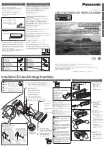
1-8-5
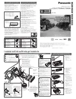
Audio Block Diagram
E5K50BLA
A
V
CB
A
BD MAIN CB
A
AUDIO SIGNAL
IC7001
(A
UDIO D/A CONVER
TER)
A
UDIO
DA
C
3
4
5
8
2
7
6
(L-CH)
(R-CH)
1
R-CH
MUTE
L-CH
MUTE
16
14
15
A
U
DIO(L)-
OUT
A
U
DIO(R)-
OUT
Q2203
MUTE-ON
Q2202
MUTE-ON
Q2200
DRIVE
Q2201
DRIVE
JK2200 (REAR)
IC2200
(OP AMP)
7
1
6
2
24
24
A
UDIO(L)
22
22
A
UDIO(R)
26
26
A
UDIO(L)-MUTE
25
25
A
UDIO(R)-MUTE
55
SPDIF
CN7101
C
N2001
DIGIT
A
L
A
U
DIO OUT
(CO
AXIAL)
T
O
SYSTEM CONTR
O
L
BLOCK DIA
GRAM
A
UDIO-MUTE
T
O
DIGIT
A
L
SIGNAL
PR
OCESS 2
BLOCK DIA
GRAM
MC
MD
D
A
C-SCK
D
A
C-BCK
D
A
C-LRCK
MS1
DA
T
A
SPDIF
DIGIT
AL
A
UDIO OUT
(OPTICAL)
JK2100
(REAR)
JK2400 (REAR)
B
U
FFER
Q2100
Содержание DV-BD507BCDC1N
Страница 3: ...1 1 1 E5K50SP SPECIFICATIONS...
Страница 13: ...1 5 3 E5K50DC 11 AV CBA 13 Shield Bracket 14 SD PCB Bracket S 13 S 14 S 11 S 12 12 Power Holder Fig D5...
Страница 27: ...1 9 4 AV 2 3 Schematic Diagram E5K50SCAV2...
Страница 28: ...1 9 5 AV 3 3 Schematic Diagram E5K50SCAV3...
Страница 29: ...1 9 6 Front Power SW Schematic Diagram E5K50SCF...
Страница 30: ...1 9 7 E5K50SCSD SD A SD B SD C Schematic Diagram...
Страница 38: ...1 9 15 BD Main 8 11 Schematic Diagram E5K50SCBD8...
Страница 40: ...1 9 17 BD Main 10 11 Schematic Diagram E5K50SCBD10...
Страница 54: ...DV BD507 B CDC1N E5K50UD 2009 06 19...