40055101TH Rev.4
370 /
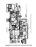
(3) G3 receive Mode
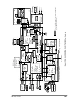
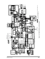
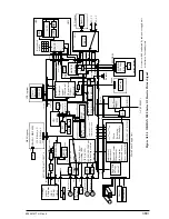
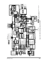
Figure A2.1.3 (For OKIOFFICE 44/OKIFAX 4100)/Figure A2.2.3 (For OKIFAX 5000 series)
show the G3 receive picture signal route
In the G3 mode, the high-speed picture signal arriving from the telephone line at L1 and L2 of
NCU passes through the transformer T1 and the amplifier and is input to the MODEM as “R”
signal. After demodulation by modem, the picture data is sent to CPU. The CPU performs the
picture data processing (decode) for this picture data and stores into the DRAM. Then, the stored
picture data is again written into DRAM (as a page memory) by the picture processing control of
CPU. When the data for one page has been stored in the DRAM/P-SRAM, the data is read out
from the DRAM and sent to IOGA. The picture data is converted into a signal data by the printer
control of IOGA and transferred to the LED print head for printing as HDATA 0/1.
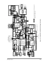
(4) 300bps Send Mode
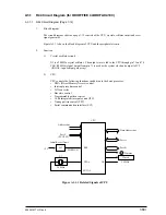
Figure A2.1.4 (For OKIOFFICE 44/OKIFAX 4100)/Figure A2.2.4 (For OKIFAX 5000 series)
show 300bps send protocol signal route
In G3 communication, this is the route of the procedural control signals (pre-message, post-
message phases etc.) at 300bps.
The protocol send data is read into DRAM in the sequence the contents of varrious data stored in
the FLASH memory area in advance under the control of CPU. The contents of the frame has
been edited on the DRAM by CPU and sent to MODEM via CPU. HDLC (high level data link
control) frame of the data is structured by the modem and converted to serial data in synchrony
with the modem’s DCLK (data clock). After modulation, the protocol signal is output from “S” of
the modem and sent to the telephone line L1 and L2 via the transformer T1 of NCU.
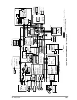
(5) 300bps Receive Mode
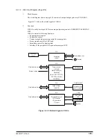
Figure A2.1.5 (For OKIOFFICE 44/OKIFAX 4100)/Figure A2.2.5 (For OKIFAX 5000 series)
show 300bps receive protocol signal route.
In G3 communication, this is the route of the procedural control signals (pre-message, post-
message phases etc.) at 300bps.
The 300bps modulated signals received via the telephone line L1 and L2 of the NCU are sent from
pin R to Pin RXA1 of the modem. After demodulation by the modem, the demodulated digital
signals are sent to the CPU via the data bus from the modem. The data is read and decoded by the
CPU and written into the DRAM. The written data is interpreted according to bit assigment of the
binary procedural signals in the ITU recommendations. The successive modes of communication
(for example, line density,encoding scheme, etc.) are determind.
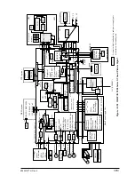
(6) Report Printing
This signal route describes the printing route of character data used to print Activity Report,
Message Confirmation Report, etc.
The report data is read into DRAM in the sequence the contents of data stored in the FLASH
memory in advance under the control of CPU. The contents of data is edited on the DRAM. The
data is read out from the DRAM and sent to IOGA. The data is converted into a serial data by the
picture control of IOGA and transferred to the LED print head for printing as HDATA 0/1.
Содержание B4100
Страница 73: ...40055101TH Rev 4 73 2 For OKIFAX 5000 series AC Power Switch AC Inlet FX050VP C2 014...
Страница 158: ...40055101TH Rev 4 158 Appearance of the OKIOFFICE44 OKIFAX 4100 FX048 CP4 1 Fig 01...
Страница 461: ...40055101TH Rev 4 461...
Страница 462: ...40055101TH Rev 4 462...
Страница 463: ...40055101TH Rev 4 463...
Страница 464: ...40055101TH Rev 4 464...
Страница 465: ...40055101TH Rev 4 465...
Страница 466: ...40055101TH Rev 4 466...
Страница 467: ...40055101TH Rev 4 467...
Страница 468: ...40055101TH Rev 4 468...
Страница 469: ...40055101TH Rev 4 469...
Страница 470: ...40055101TH Rev 4 470...
Страница 471: ...40055101TH Rev 4 471...
Страница 472: ...40055101TH Rev 4 472...
Страница 473: ...40055101TH Rev 4 473...
Страница 545: ...40055101TH Rev 4 545 54 SECTION 1 CABINET ASSEMBLY FAX NIP FX048...
Страница 548: ...40055101TH Rev 4 548 SECTION 2 UNIT PRINTER...
Страница 550: ...40055101TH Rev 4 550 SECTION 3 UNIT 048 OPE PANEL...
Страница 552: ...40055101TH Rev 4 552 SECTION 4 OPEPANEL OPERATION PANEL ASSEMBLY...
Страница 554: ...40055101TH Rev 4 554 SECTION 5 FRAME ASSEMBLY SCANNER L...
Страница 556: ...40055101TH Rev 4 556 SECTION 6 PLATE ASSEMBLY SCANNER B...
Страница 558: ...40055101TH Rev 4 558 SECTION 7 PLATE ASSEMBLY SCANNER R...
Страница 560: ...40055101TH Rev 4 560 17 16 15 10 SECTION 8 FRAME ASSEMBLY SCANNER U...
Страница 562: ...40055101TH Rev 4 562 13 SECTION 9 COVER ASSEMBLY TOP...
Страница 564: ...40055101TH Rev 4 564 SECTION 10 PLATE ASSEMBLY BASE...
Страница 569: ...40055101TH Rev 4 569 SECTION 12 PRINTER HEAT ASSY...
Страница 571: ...40055101TH Rev 4 571 SECTION 13 CABLES...
Страница 574: ...40055101TH Rev 4 574 SECTION 1 CABINET ASSEMBLY...
Страница 576: ...40055101TH Rev 4 576 SECTION 2 CONTROL PANEL ASSEMBLY OKIFAX 5200 5300...
Страница 577: ...40055101TH Rev 4 577 SECTION 2 CONTROL PANEL ASSEMBLY OKIFAX 5500 5600...
Страница 579: ...40055101TH Rev 4 579 SECTION 3 PRINTER ASSEMBLY...
Страница 582: ...40055101TH Rev 4 582 SECTION 4 BASE ASSEMBLY 30 37 38...
Страница 585: ...40055101TH Rev 4 585 SECTION 5 SCAN UNIT...
Страница 587: ...40055101TH Rev 4 587 SECTION 6 PAPER GUIDE U ASSEMBLY...
Страница 589: ...40055101TH Rev 4 589 SECTION 7 CABLES 10...
Страница 591: ...40055101TH Rev 4 591 SECTION 8 OPTION TELEPHONE US...
Страница 594: ...40055101TH Rev 4 594 SECTION 8 OPTION TELEPHONE UK ITA NOR DEN BEL...
Страница 597: ...40055101TH Rev 4 597 SECTION 8 OPTION TELEPHONE HOL GER FRA SWITZ AUT INT L...
Страница 615: ...40055101TH Rev 4 615 5 2 PCB Layout TQSB 2PCB PU FG CONTROLLER MOTOR DRIVER SEN2 MOTOR OSC SEN1...
Страница 616: ...40055101TH Rev 4 616 Figure 6 1 6 PARTS LIST SECTION1 CABINET CASSETTE ASSEMBLY 7 2 8 1 6 5 3 4 O P...
Страница 617: ...40055101TH Rev 4 617 SECTION2 MECHANICAL ASSEMBLY Figure 6 2 0 D A E C K B L 9 M F H N G R Q S T U V J I B A B A...


