3.
Slide the 5420 into the Octagon card cage. The components on
the card should face to the left or upward depending on the
type of card cage.
4.
Power on your system.
5.
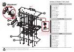
Refer to Figure 3 for a functional diagram of the 5420 card:
PC Bus
65530 SVGA
Controller
82C404
Clock
Decode
29C256
Ext
BIOS
DC-DC
Converter
50-position IDC
J1
DB-15
J2
Y1
14-318
MHz
R6 DC
Adj
Flat Panel Data
Analog VGA
Data
Address
Display
Memory
Filter
W2
W4
DC Polarity
See, page 9
W3
Figure 3—5420 Functional Diagram
5420 Super VGA Video Card – 4
Содержание 5420
Страница 2: ......
Страница 3: ......
Страница 4: ......
Страница 5: ......
Страница 6: ......
Страница 7: ......
Страница 8: ......
Страница 9: ......
Страница 10: ......
Страница 11: ......
Страница 12: ......
Страница 13: ......
Страница 14: ......
Страница 15: ......
Страница 16: ......
Страница 17: ......
Страница 18: ......
Страница 19: ......
Страница 20: ......
Страница 21: ......
Страница 22: ......
Страница 23: ......
Страница 27: ...5420 Super VGA Video Card 20 This page left intentionally blank ...