


UM10412
All information provided in this document is subject to legal disclaimers.
© NXP B.V. 2010. All rights reserved.
User manual
Rev. 1 — 2 November 2010
4 of 26
NXP Semiconductors
UM10412
UBA2021 evaluation board
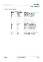
3. Board
description
The board consists of two separate PCBs. The main board with the resonance circuit and
a small daughter board with the UBA2021 IC.
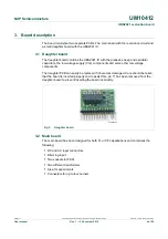
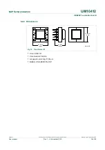
3.1 Daughter
board
The daughter board contains the UBA2021 IC with the preheat, sweep and oscillator
capacitors, the low voltage supply (V
DD
) components and some other low voltage
components.
The daughter PCB can easily be replaced if it becomes damaged. Care should be taken
that the board is inserted properly and to assist this, pin 11 has been removed from the
daughter board to prevent inserting the board incorrectly.
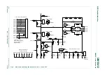
3.2 Main
board
The main board has been designed for both TL or CFL applications and comprises the
following:
•
DC and AC input connectors
•
Dimming input
•
Two sockets for FETs
•
Two different transformers
•
Area for experiments
•
Connectors for up to four burners
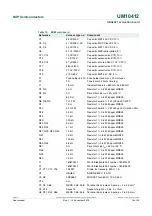
Fig 2.
Daughter board
019aaa283