NXP Semiconductors UBA2021 Скачать руководство пользователя страница 23

xxxxxxxxxxxxxxxxxxxxx xxxxxxxxxxxxxxxxxxxxxxxxxx xxxxxxx x x x xxxxxxxxxxxxxxxxxxxxxxxxxxxxxx xxxxxxxxxxxxxxxxxxx xx xx xxxxx 
xxxxxxxxxxxxxxxxxxxxxxxxxxx xxxxxxxxxxxxxxxxxxx xxxxxx xxxxxxxxxxxxxxxxxxxxxxxxxxxxxxxxxxx xxxxxxxxxxxx x x 
xxxxxxxxxxxxxxxxxxxxx xxxxxxxxxxxxxxxxxxxxxxxxxxxxxx xxxxx xxxxxxxxxxxxxxxxxxxxxxxxxxxxxxxxxxxxxxxxxxxxxxxxxx xxxxxxxx 
xxxxxxxxxxxxxxxxxxxxxxxxx xxxxxxxxxxxxxxxxxxxx xxx

UM10

412

Al

l i

n

for
m

at

ion
 pr
ovi
ded

 in 
this

 do

cum

ent i

s

 sub

jec
t to 

leg
a

l d
is

c

la

im
er

s.

©

 NXP

 B.V

. 2010.

 Al
l r

ig

h

ts

 r

e

s

e

rv

ed.

User m

a

nu
al

Rev

. 1

 — 2 No

vemb

e

r 2010 

23 o

f 26

N

X

P Semi

conductor

s

UM10412

UBA202

1 ev

aluat

io

n

 boar

d


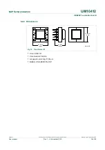
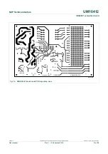
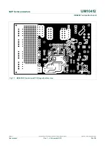
Fig 18. UBA2014/21 main board silk screen top view

019aaa294

X65

X56

1

LAMP 1

X66

EXPERIMENTING AREA

15 

μ

H

15 

μ

H

4 mH

2 mH

2.5 mH

3 mH

3.5 mH

SH

SH

GND

GND

GND

SH

SH

SH

TRAFO 1

LAMP CURRENT SENSE

PREHEAT CURRENT SENSE

GND

GND

PCS

2021

VCC

GND

GL

VBRG

PCS

GH

SH

LVS

VREF

CSP

CSN

UBA20 (14/21)  Daughter Board

High
Side
FET

Low
Side
FET

HALF

BRIDGE

WWW.NXP.COM
UBA20 (14/21)
DEMO BOARD
V1.2

GND

GND

GND

High Voltages
On This Board !

X64

X63

X61

X60

X58

X57

X54

X53

X52

X70

X72

X74

X76

X91

X50

X67

X117

X69

X73

X75

X77

X48

X47

X45

X109

X44

X43

X40

X37

X36

X35

X31

X29

X28

X26

X25

X23

X22

X19

X18

X17

X15

X105

X113

1

1

T2

T3

1

1

2

2

3

3

4

4

5

5

10

10

9

9

8

8

7

7

6

6

X106

X107

X108

X96

X103

X103

V16

X115

R37

R39

R38

12

11

1

1

1

1

1

1

2

R9

V1

X1

C16

C15

R33

R27

R29

R34

R8

C14

R40

V15

R19

R18

X68

X34

X32

R6

R32

R31

6

5

X39

7

8

T1

R4

X114

R7

V11

V12

C12

C17

R10

X33

C11

C18

R5

R3

X14

R36

X2

R35

1

1

1

g

d

s

g

d

s

R20

R1

L1

V2

C3

C2

X3

F1

X120

X88

X87

X85

X83

X81

X79

X89

X104

X78

X80

X82

X84

X86

C5

C4

R22

R24

R2

R23

R25

C1

C6

GND

WW/YY

ANALOG DIM IN

VDC_IN = 400 V

230  VAC  50 Hz

2 A/T

0 - 10 V

X102

X94

X92

X90

X62

X59

X55

X49

X42

1

LAMP 2

1

1

X46

X41

X38

X30

X21

1

LAMP 3

X27

X24

X20

X13

X8

1

LAMP 4

X11

X9

X6

X112

1

X111

1

X110

1


Содержание UBA2021

Страница 1: ...UBA2021 evaluation board Rev 1 2 November 2010 User manual Document information Info Content Keywords UBA2021 evaluation board TL CFL Abstract This document is the user manual for the UBA2021 evaluati...

Страница 2: ...served User manual Rev 1 2 November 2010 2 of 26 Contact information For more information please visit http www nxp com For sales office addresses please send an email to salesaddresses nxp com NXP Se...

Страница 3: ...CFL applications To optimize flexibility almost no protection is build in except for IC internal protection The board does not conform with any safety norm CAUTIONS Do not supply voltages to the boar...

Страница 4: ...preheat sweep and oscillator capacitors the low voltage supply VDD components and some other low voltage components The daughter PCB can easily be replaced if it becomes damaged Care should be taken...

Страница 5: ...ocument is subject to legal disclaimers NXP B V 2010 All rights reserved User manual Rev 1 2 November 2010 5 of 26 NXP Semiconductors UM10412 UBA2021 evaluation board Fig 3 UBA2014 21 Main board with...

Страница 6: ...preheat time of 1 85 s Fig 4 Daughter board with UBA2021 circuit 019aaa284 30 k R3 C1 A1 100 nF C2 330 nF 16 V C3 100 pF 1 2 47 R4 2 1 150 k R1 1 2 150 k R2 1 2 160 k R8 1 2 2 1 2 1 2 CI 13 1 14 RHV...

Страница 7: ...r 2 X115 header 2 X2 socket 3 1 2 C5 33 nF 100 V 1 2 47 k R25 1 2 D placed in header V6 2SK3569 S G D placed in header V3 2SK3569 S G Y5 jumper C6 4 7 nF 2000 V 1 2 C19 470 nF 63 V 1 CSN 1 2 3 2 C17 6...

Страница 8: ...1 1 2 1 4 2 3 2 C3 47 nF 305 Vac 1 2 C2 47 nF 305 Vac 1 1 1 2 2 2 X1 VAC In 230 V 50 Hz VDC In 400 V MKDS 2 5 2 5 08 1 2 Fig 7 Main board dimming input only in combination with UBA2014 daughter board...

Страница 9: ...08 1 1 1 X6 TP 2 Y3 jumper Y1 jumper Y4 jumper Y2 jumper 1 2 X9 TP 1 3 X11 TP 1 4 X13 TP X21 LAMP 3 MKDS 2 2 4 5 08 1 1 X20 TP 1 2 X24 TP 1 3 X27 TP 1 4 X30 TP X42 LAMP 2 MKDS 2 2 4 5 08 1 1 X38 TP 1...

Страница 10: ...input The UBA2021 does not have dimming functionality so this input is not used If dimming is required please use the UBA2014 5 3 Lamp connectors There are four lamp connectors on the board The connec...

Страница 11: ...P Comment X6 connection for filament 1 X9 connection for filament 1 X11 connection for filament 2 X13 connection for filament 2 Table 7 Connections of the daughter board Test Pin Name Comment X78 CSN...

Страница 12: ...e rather than by the lamp current or the half bridge current 5 7 1 Half bridge current sensing The half bridge current is sensed for controlling the preheat current Different values of the sense resis...

Страница 13: ...of the transformer Table 11 shows the different inductance values The specifications of the transformer are listed in Section 6 Transformer T3 has a double footprint that enables the use of different...

Страница 14: ...valent Bobbin RM 8 12 pin vertical type Fig 10 Transformer T1 schematic diagram 019aaa301 N3 10 12 7 9 6 1 N2 N1 Table 13 Electrical characteristics for transformer T1 Properties Test conditions Value...

Страница 15: ...matic diagram 019aaa302 N7 9 10 7 8 6 1 2 N6 N1 N2 3 N3 4 N4 5 N5 Table 14 Electrical characteristics for transformer T3 Properties Test conditions Value Unit Tolerance InductanceN1 N5 50 kHz 0 1 V L0...

Страница 16: ...All rights reserved User manual Rev 1 2 November 2010 16 of 26 NXP Semiconductors UM10412 UBA2021 evaluation board 6 2 2 Dimensions Core E30 15 7 Core material Ferrite Air gap in center leg 1100 m Bob...

Страница 17: ...ault settings Jumper Position Comment X32 short half bridge sense resistor 1 used for PCS X34 open X33 1 2 open 2 3 short use lamp current sensing X114 short connect transformer T1 X115 short X39 1 2...

Страница 18: ...50 V 1 C5 n m C6 470 pF 500 V Capacitor ceramic 500 V NP0 5 C7 1 F 25 V Capacitor ceramic X7R 25 V 10 C8 1 nF 100 V Capacitor ceramic X7R 100 V 10 C9 10 n Capacitor ceramic X7R 50 V 10 C10 2 2 n 100 V...

Страница 19: ...5 C R5 8 2 K Resistor 1 0 6 W 50 ppm MRS25 R6 R8 R9 1 2 W Resistor Power 5 2 W 100 ppm C MFP R7 1 K Resistor 1 0 6 W 50 ppm MRS25 R10 33 2 W Resistor Power 5 2 W 450 ppm C Carbon Film R18 33 k Resisto...

Страница 20: ...2 November 2010 20 of 26 NXP Semiconductors UM10412 UBA2021 evaluation board 9 Layout Top view Bottom view Fig 14 Daughter PCB layout 019aaa291 T 019aaa290 R1A Top view Bottom view Fig 15 Daughter boa...

Страница 21: ...subject to legal disclaimers NXP B V 2010 All rights reserved User manual Rev 1 2 November 2010 21 of 26 NXP Semiconductors UM10412 UBA2021 evaluation board Fig 16 UBA2014 21 main board PCB layout top...

Страница 22: ...cument is subject to legal disclaimers NXP B V 2010 All rights reserved User manual Rev 1 2 November 2010 22 of 26 NXP Semiconductors UM10412 UBA2021 evaluation board Fig 17 UBA2014 21 main board PCB...

Страница 23: ...CURRENT SENSE GND GND PCS 2021 VCC GND GL VBRG PCS GH SH LVS VREF CSP CSN UBA20 14 21 Daughter Board High Side FET Low Side FET HALF BRIDGE WWW NXP COM UBA20 14 21 DEMO BOARD V1 2 GND GND GND High Vo...

Страница 24: ...10 All rights reserved User manual Rev 1 2 November 2010 24 of 26 NXP Semiconductors UM10412 UBA2021 evaluation board 10 Glossary CFL Compact Fluorescent Lamp MOSFET Metal Oxide Semiconductor Field Ef...

Страница 25: ...operating safeguards to minimize the risks associated with their applications and products NXP Semiconductors does not accept any liability related to any default damage costs or problem which is base...

Страница 26: ...4 3 2 Main board 4 4 Schematics 6 5 Connectors 10 5 1 Power supply connectors 10 5 2 Dimming input 10 5 3 Lamp connectors 10 5 4 Test points 11 5 5 Transformer T1 12 5 6 FET 12 5 7 Current sense sele...

Отзывы: