


NXP Semiconductors
UM11711
PCAL6524EV-ARD evaluation board
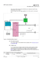
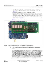
4.2 Kit featured components
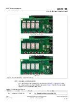
identifies the main components on the board. The main elements are called out
in the picture. The Arduino port connectors (J1, J2, J3, J4) are located on the bottom side
of the board.
Figure 1. PCAL6524EV-ARD board, top view (up) and bottom view (down)
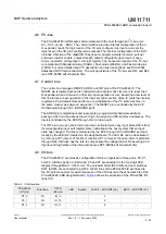
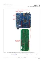
4.3 Block diagram
shows a block diagram of the PCAL6524EV-ARD daughterboard. Alongside the
DUT (U1), the board includes a series of peripherals that assures the operation of the
board. U1 is linked to Arduino interface (J1 to J4) through two busses: the I
2
C-bus and
the control bus.
The port P0 and P1 (8-bit wide each) controls the four-digit LED display (D9 to D12)
located on the board, through the MAX V CPLD which acts as display decoder/driver. Al
sixteen I/O lines are shared with the 16 BIT I/O PORT (J6).
The port P2 (8-bit wide) is shared with the on-board user LEDs D5 to D8, user switches
SW1 to SW4, and the 8 BIT I/O PORT (J7). The first four LSB I/O lines of the port P2
UM11711
All information provided in this document is subject to legal disclaimers.
© NXP B.V. 2022. All rights reserved.
User manual
Rev. 1.0 — 19 January 2022
6 / 30