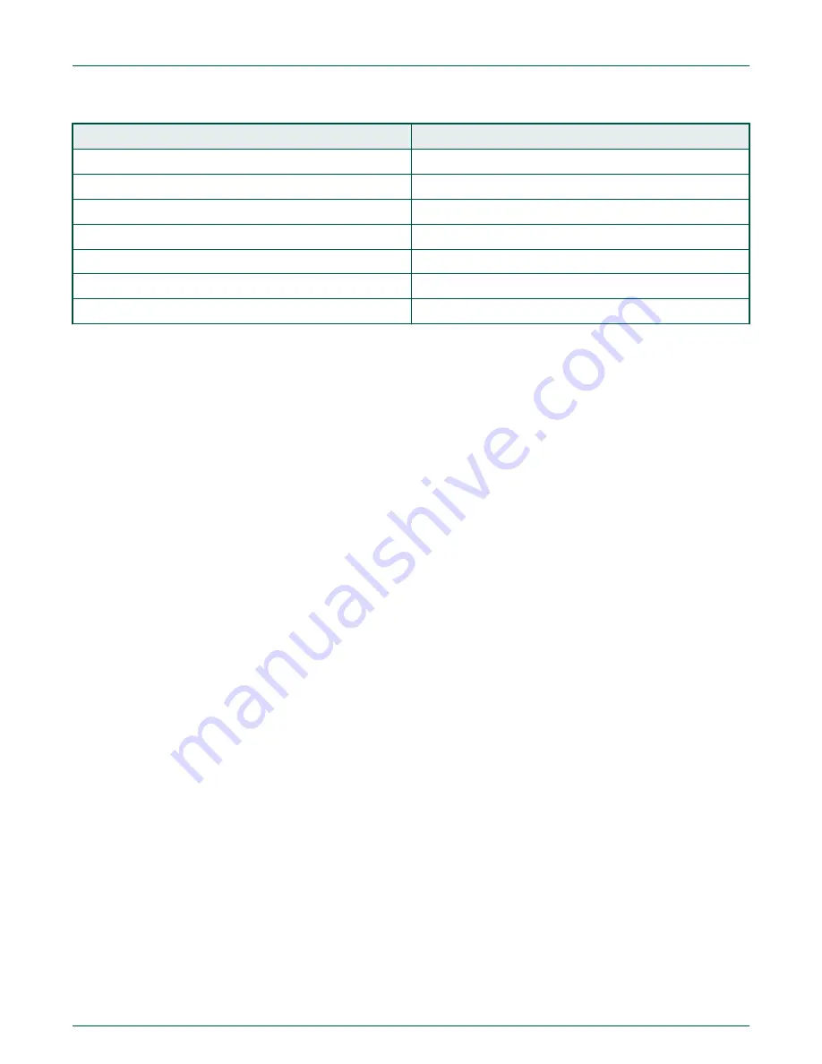
NXP Semiconductors i.MX RT685 Скачать руководство пользователя страница 18

Table 4. PMIC pins

PMIC

IMXRT685

SCL

PMIC_I2C_SCL

SDA

PMIC_I2C_SDA

MODESEL0

PMIC_MODE0

MODESEL1

PMIC_MODE1

INT

PMIC_IRQ_N

SYSREST

RESET

ON

SW4 (JP16, 1-2)

For further information, please refer to the board schematic.

NXP Semiconductors

Board power

i.MX RT685 Evaluation Board, Rev. 0, March 20 2020

User's Guide

18 / 31

Содержание i.MX RT685

Страница 1: ...i MX RT685 Evaluation Board NXP Semiconductors Document identifier UM11159 User s Guide Rev 0 March 20 2020...

Страница 2: ...l connections 19 6 1 USB high speed port 19 6 2 USART header 19 6 3 I3C header 19 6 4 Flexcomm header 19 6 5 Additional expansion header 21 Chapter 7 On board peripherals 22 7 1 Audio Codec 22 7 2 Aud...

Страница 3: ...85 EVK includes the following features i MX RT685 Cortex M33 core processor with Cadence Xtensa HiFi4 DSP Onboard high speed USB Link2 debug probe with CMSIS DAP protocol supporting Cortex M33 debug o...

Страница 4: ...nectors NXP FXOS8700CQ accelerometer Stereo audio codec with line in out and electret microphone Stereo NXP TFA9894 digital amplifiers with option for external 5V power for higher performance speakers...

Страница 5: ...ons and headers Table 1 provides a description of connectors LEDs and buttons Table 1 Connectors LEDs buttons and headers Circuit ref Rev E Description Default Reference D1 Reset LED N A Schematic D2...

Страница 6: ...ce pins N A Schematic J11 J20 Screw terminal connections for external speakers When attaching a speaker ensure that the appropriate driver settings are used in the TFA9894 devices to avoid damage to t...

Страница 7: ...sion connector Arduino reset if JP14 is installed N A Reset SW4 PMIC on button N A PMIC ON SW5 Boot Config switch ISP boot mode selection Switch the DIP switch for ISP port signal to ON to pull that p...

Страница 8: ...setting to reprogram the Link2 internal flash with a new image using the LPCScrypt utility or to use the MCUXpresso IDE with CMSIS DAP protocol The Link2 flash is pre programmed with a version of CMS...

Страница 9: ...ers 2 3 digital amplifiers Audio Codec and Audio digital amplifiers JP7 JP8 I2S data select for audio devices controlling which audio device drives the I2S connections to the i MX RT685 I2S port Inser...

Страница 10: ...lect ISP1 P1 16 Schematic JP14 Reset enable disable to Arduino Install jumper to route the i MX RT685 reset control signal to the standard Arduino reset pin Open Schematic JP15 Power supply to FXOS870...

Страница 11: ...ply current and Schematic JP27 This jumper is provided for optional insertion of an ammeter to measure supply current to the i MX RT685 VDDIO_2 supply pins Closed Measuring MIMXRT685 EVK device supply...

Страница 12: ...round N A Schematic J35 Host reset control header Provides a connection point for an external host to drive the reset of the i MX RT685 and other devices sharing this reset Open Schematic J38 Footprin...

Страница 13: ...ate compatible firmware image is used with the MCUXpresso IDE If the Debug Probe is set up to boot in DFU mode the USB bridge functions virtual COM port and Debug Probe features will not be available...

Страница 14: ...n Interface Devices CMSIS DAP LPC SIO two HID Compliant Devices and a USB Input Device one under Ports LPC LinkII UCom Your board is now ready to use with your 3rd party tool Follow the instructions f...

Страница 15: ...ties are available for free download at https www nxp com lpcscrypt The CMSIS DAP firmware image installed at the factory and by LPCScrypt will uniquely identify itself to the host computer so that mo...

Страница 16: ...the search bar In the Device Manager under Ports the LPC LinkII UCom Port device and its name should be visible This VCOM port will only appear if the Debug Probe has been programmed with the CMSIS DA...

Страница 17: ...efer to Power Sequencing in the device data sheet 5 1 Measuring MIMXRT685 EVK device supply current Current supply to the RT685 Core can be measured via JP29 VDDCORE The voltage supplied can be measur...

Страница 18: ...MIC_I2C_SDA MODESEL0 PMIC_MODE0 MODESEL1 PMIC_MODE1 INT PMIC_IRQ_N SYSREST RESET ON SW4 JP16 1 2 For further information please refer to the board schematic NXP Semiconductors Board power i MX RT685 E...

Страница 19: ...Host Controller on the User Manual 6 2 USART header Header J16 is provided as a convenient way to use the USART with a serial to USB cable Flexcom 0 ports P0_1 and P0_2 are used for this feature since...

Страница 20: ...Figure 4 i MX RT685 EVK Flexcomm pinout NXP Semiconductors Board serial connections i MX RT685 Evaluation Board Rev 0 March 20 2020 User s Guide 20 31...

Страница 21: ...J1 Table 5 Additional header port pinout Header pin Port Pin 1 P2_11 Pin 2 P2_13 Pin 3 P0_3 Pin 4 P2_12 Pin 5 P0_4 Pin 6 P0_13 Pin 7 P0_12 Pin 8 P2_15 Pin 9 P2_14 Pin 10 P0_11 NXP Semiconductors Boar...

Страница 22: ...t I2C SDA P2_30 I2C SCL P2_29 I2S BLCK P0_7 I2S DAI P0_9 I2S DAO P0_23 I2S WS P0_8 CODEC MCLK P1_10 There are three jumpers JP6 JP7 and JP8 to select IMXRT685 I2S connections lines between Codec and a...

Страница 23: ...he board includes an NXP FXOS8700CQ accelerometer interfaced to port 0 P0_17 and P0_18 with its interrupt output connected to P1_5 JP30 has to be populated The accelerometer has an I2C address of 0b00...

Страница 24: ...a SD card device connected to SDIO 1 interface The RT6xx will look for a valid image in the SD card device If there is no valid image found the RT6xx will enter the ISP boot mode based on OTP DEFAULT...

Страница 25: ...OTP external Flash SD or eMMC device 111 High High High Serial Master boot SPI Slave I2C Slave or UART USB HID is used to download a boot image over the serial interface SPI Slave I2C Slave or UART US...

Страница 26: ...d You must move R379 2 3 and R380 2 3 to use this header For further details refer to the board schematics Table 11 External DMIC connections Circuit reference Port PDM_CLK01_Ext Not connected by defa...

Страница 27: ...ircuit reference Port Pin 1 P1_14_SPI_SS0_A P1_14 Pin 2 BRIDGE_INTR_ISP P1_16 JP13 Pin 3 P1_13_SPI_MOSI_A P1_13 Pin 4 P0_3 P0_3 Pin 5 P1_12_SPI_MISO_A P1_12 Pin 6 P0_15_FC2_SCL P0_15 Pin 7 P1_11_SPI_C...

Страница 28: ...Figure 5 i MX RT685 EVK Arduino J27 and J28 headers pinout NXP Semiconductors Expansion connectors i MX RT685 Evaluation Board Rev 0 March 20 2020 User s Guide 28 31...

Страница 29: ...Figure 6 i MX RT685 EVK Arduino J29 and J30 headers pinout NXP Semiconductors Expansion connectors i MX RT685 Evaluation Board Rev 0 March 20 2020 User s Guide 29 31...

Страница 30: ...in 1 for the negative reference and JP10 pin 2 for the positive reference If jumpers are populated on both connectors the positive reference will be connected to SW2_OUT 1 8 by default and it can be r...

Страница 31: ...te design and operating safeguards to minimize the risks associated with their applications and products NXP the NXP logo NXP SECURE CONNECTIONS FOR A SMARTER WORLD COOLFLUX EMBRACE GREENCHIP HITAG I2...

Отзывы: