


NXP Semiconductors
IMXRT500HDG
i.MX RT500 Hardware Design Guide
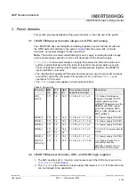
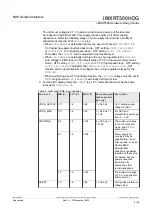
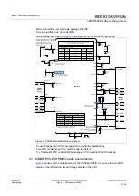
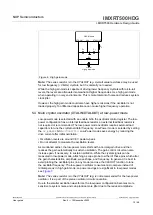
2. PMIC mode pins are the outputs that are controlled by an always-on supply. These
pins must have external pullups to
VDD_AO1V8
and get validated after several
microseconds once VDD_AO1V8 is stable.
3. The
VDDA_ADC1V8
supply and
VREFP
reference are powered-up at the same time as
VDD1V8
or later.
4. The
VDDIO
rails and
VDDA_BIAS
are also powered at the same time as
VDD1V8
or
later.
CAUTION:
When
VDDIO_3
is 3.0 V, there must be a delta of not more than 1.89 V
during the rampup.
5.
VDDCORE
is powered last by the PMIC, which handles the power sequencing.
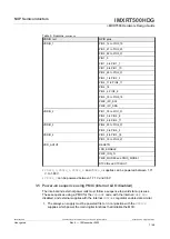
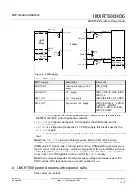
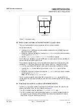
Note:
When
LDO_ENABLE
is externally tied low, the user must boot at
VDDCORE
=
1.0 V or higher (Low-power / Normal clock mode - OTP setting -
BOOT_CLK_SPEED
)
or
VDDCORE
= 1.13 V (High-Speed clock - OTP setting -
BOOT_CLK_SPEED
).
Thereafter, the
VDDCORE
can be adjusted to the desired level. The PMIC also
provides the
RESETN
deassertion after
VDDCORE
is stable.
When a PMIC is not used, enable the internal
VDDCORE LDO
to provide
VDDCORE
. The
PMC releases
RESETN
internally when
VDDCORE
is stable.
Note:
For ERR050716, generally, all 1.8 V power pins are supplied by the same
regulator, so all are applied at the same relative time. Decoupling capacitor charging
delays are not considered to be significant when all the 1.8 V domains are powered at
the same time.
IMXRT500HDG
All information provided in this document is subject to legal disclaimers.
© 2022 NXP B.V. All rights reserved.
User guide
Rev. 0 — 15 November 2022
8 / 48


