


NXP Semiconductors
IMXRT500HDG
i.MX RT500 Hardware Design Guide
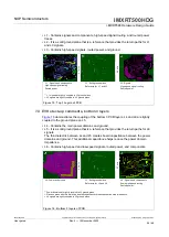
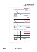
Figure 25. EVK external memory layouts
•
Octal flash: Most data and control lines are routed on L1, it is good because all the HS
signals between MCU and memory must be on the same layer. The MCU and memory
can be on different layers, but all the HS signals should be on one layer.
•
Matched signal lengths: It is good and required for high-speed bus signal integrity to
match signal lengths, layer routing, and matched vias.
•
L2 ground reference for impedance control: It is good since all the HS signals should
have a ground plane for return currents.
•
Several data lines are routed on L1 and L3: It is poor since all HS signals between
MCU and memory should be on the same layer.
•
Shorting resistors for shared components and signals: It is poor because these
options create stubs and interfere with impedance control. However, these options
are necessary to demonstrate the functionality of multiplexed functions on an
evaluation board. Shorting resistors must be used in a development environment, not in
production.
Note:
This interface uses the
FLEXSPI0
bus which is shared with the QSPI flash
memory on the EVK.
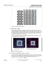
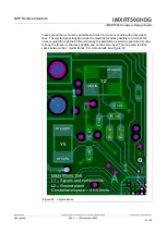
7.16 EVK memories QSPI flash (U37)
Continuing to look at good and poor design practices as fallows, for more details, see
and
IMXRT500HDG
All information provided in this document is subject to legal disclaimers.
© 2022 NXP B.V. All rights reserved.
User guide
Rev. 0 — 15 November 2022
36 / 48


