


IMXRT500HDG
i.MX RT500 Hardware Design Guide
Rev. 0 — 15 November 2022
User guide
Document information
Information
Content
Keywords
IMXRT500HDG, i.MX RT500, MIMXRT595-EVK
Abstract
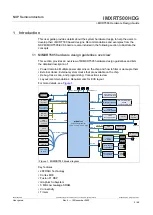
This user guide provides details about the system hardware design to help
the users to develop their i.MX RT500 based designs


