


Distributor of NXP Semiconductors: Excellent Integrated System Limited
Datasheet of MCIMX53SMD - TABLET SABRE PLATFORM MCIMX53
Contact us: [email protected] Website: www.integrated-circuit.com
Freescale Semiconductor
MCIMX53SMD Board Hardware User’s Guide, Rev. 0
29
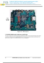
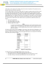
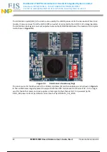
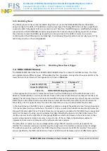
Figure 5-1.
MCIMX53SMD Board Block Diagram
5.1.
Dual LDO, DCDC, and Charger
The MCIMX53SMD board uses the MAX17085B chip as main power chip. The MAX17085B chip provides two
LDOs (3.3V and 5V), two DCDCs (3.3V and 5V), and a multi-cell Li-Ion charger. The MCIMX53SMD board
provides a three-cell Li-Ion battery as main power source. A 15V power from an external wall power supply is
connected to the MCIMX53SMD board at connector J35. The 15V supply is provided from the connector to the
MAX 17085B chip through the current protection fuse (F2).
The MAX17085B LDOs are always turned ON, when power is attached. When the ON/OFF key is pressed, the
high signal makes the MAX17085B chip to output two DCDCs (3.3V and 5V), and then power ON the PMIC. The
MAX17085B DCDCs have enough current and they are the main source of power for the whole system.
The MAX17085B chip also has charger function. When wall adapter is plugged in, 2A max charge current is fed
to the battery.
5.2.
Dialog DA9053 PMIC
The Dialog PMIC provides all regulated power to the i.MX53 processor. The PMIC is located in the middle of
the MCIMX53SMD board (near to the MAX17085B chip and i.MX53 processor). From this location, power is
supplied to the rest of the board.
When the POWER button is pressed for the first time, the MAX17085B chip outputs DCDC_3V3 and DCDC_5V,
and feeds to the PMIC. PMIC senses the Active Low signal on the nONKEY pin by RC delay circuit and begins to
power ON all voltage rails in preprogrammed sequence. The sequence is determined primarily by the order in
30 / 82
30 / 82