


KIT33905 Evaluation Boards
, Rev. 2.0
10
Freescale Semiconductor
Hardware Configuration
6.6
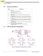
Connector J2 – SPI Control
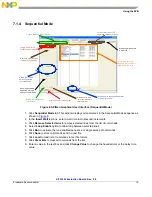
6.7
EVB – KITUSBSPIDGLEVME Interconnection
Pin #
Pin Name
Description
1
TXDC
CAN bus transmit data input. Internal pull-up to VDD
2
CSB
Chip select pin for the SPI. When the CS is low, the device is selected. In Low
Power mode with VDD ON, a transition on CS is a wake-up condition
3
INTB
This output is asserted low when an enabled interrupt condition occurs. The out-
put is a push-pull structure.
4
MISO
SPI data sent to the MCU. When the CS is high, MISO is high-impedance
5
RSTB
This is the device reset output whose main function is to reset the MCU. It has an
internal pull-up to VDD. The reset input voltage is also monitored in order to detect
external reset and safe conditions
6
MOSI
SPI data received by the device
7
NC
No Connect
8
SCLK
Clock input for the Serial Peripheral Interface (SPI) of the device
9
NC
No Connect
10
NC
No Connect
11
I_WAKE
Active high input to enable on-board FET to create a 5.0 mA load on VDD
12
NC
No Connect
13
NC
No Connect
14
NC
No Connect
15
NC
No Connect
16
GND
Ground termination
KIT33905D5EKEVBE/KIT33905BD3EVBE - J2
USB-to-SPI Dongle Board - I/O PORT
Pin #
Pin Name
Pin Name
Pin #
1
TXDC
CNTL2
2
2
CSB
CSB
1
3
INTB
CNTL1
4
4
MISO
SO
3
5
RSTB
CNTL0
6
6
MOSI
SI
5
7
NC
DATA4
8
8
SCLK
SCLK
7
9
NC
DATA3
10
10
NC
CNTL3
9
11
I_WAKE
DATA2
12
12
NC
VDD
11
13
NC
DATA1
14
14
NC
REG 3.3V
13
15
NC
DATA0
16
16
GND
GND
15