


FRDM-K28F hardware description
Freedom Board for Kinetis K28F (FRDM-K28F), User's Guide, Rev. 0, 04/2017
NXP Semiconductors
7
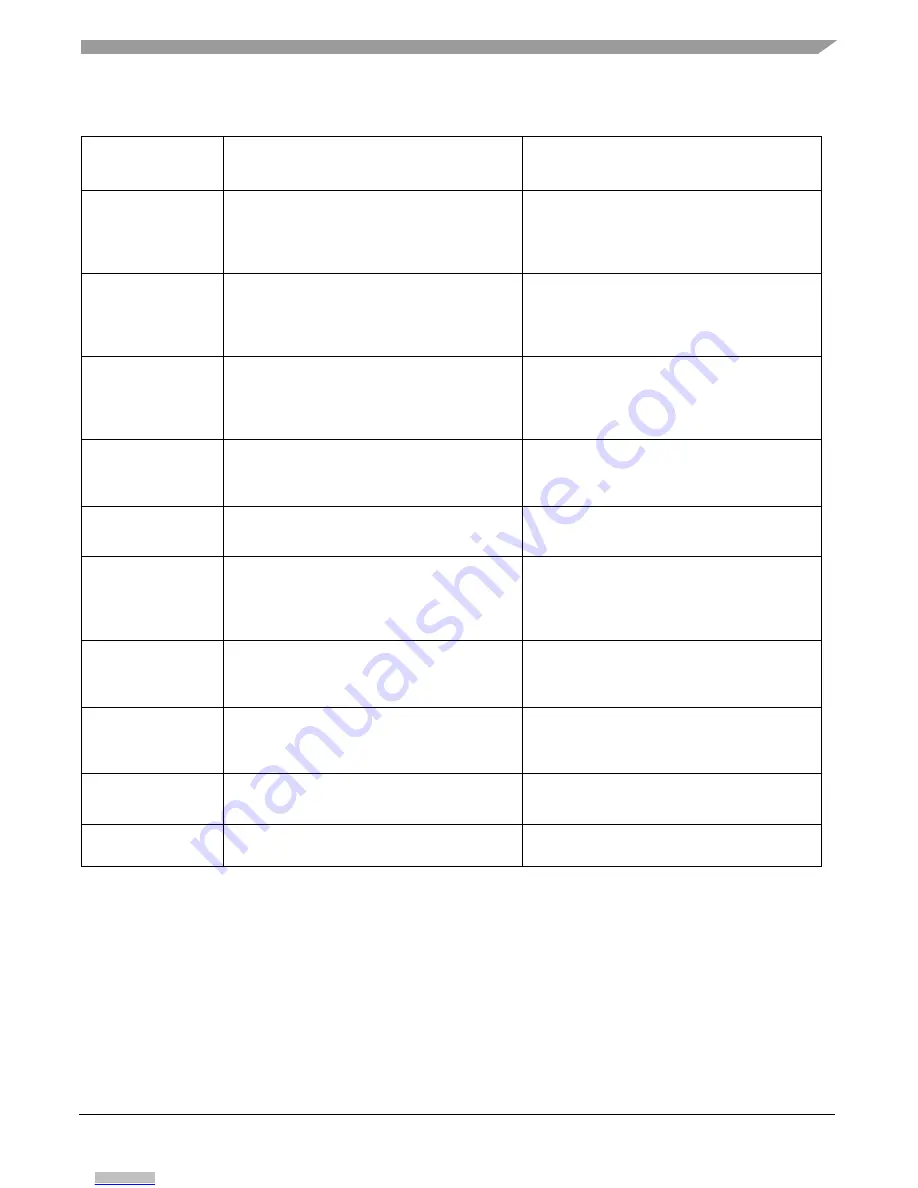
Table 2. FRDM-K28F power supplies
Power supply
name
Description
Notes
P5-9V_VIN
Power supply from the VIN pin of the I/O
headers (J3 pin 16). Sources the main 3.3 V
voltage regulator and the optional 5 V regulator
at J25. A Schottky diode provides the
back-drive protection.
—
P3V3_VREG
Regulated 3.3 V supply. Sources power to the
P3V3 supply rail. A back-drive protection
Schottky diode (D9) is provided to enable an
external 2.7 V
–3.3 V supply connection at the
J3 header P3V3 pins.
Open J26 (shorted on the bottom of the board)
if the J3 header P3V3 pins are used to supply
an alternate voltage from the on-board 3.3 V
supply.
VDD_K28F
K28F MCU voltage supply. Select the 3.3 V or
1.8 V regulator options at header J20, or the
2.7 V
–3.3 V P3V3 inputs on the J3 header.
Header J18 provides a convenient means for
energy consumption measurements.
The IS42SM16800H-6BLI SDRAM is a 3.3 V
component. Open J10 (shorted on the bottom
of the board) if the VDD_K28F node is less
than 2.7 V.
VDDIO_E_1V8
K28F VDDIO_E MCU voltage supply. Header
J15 provides a convenient means for energy
consumption measurements.
The MT25QU256ABA1EW7-0SIT QSPI flash
is a 1.8 V component. Open J16 (shorted on
the bottom of the board) if the VDDIO_E_1V8
node is ever raised above 1.8 V.
VDDCORE_1V2
K28F VDD_CORE MCU voltage supply.
Header J22 provides a convenient means for
energy consumption measurements.
—
P3V3
Main supply for the 3 V MCU VDD and
peripheral functions. Supplies nominal 3 V at
the J3 header P3V3 nodes. Sourced from the
P3V3_VREG or P3V3 inputs on the J3 I/O
header.
When the J3 P3V3 inputs are used, the voltage
must be in the 2.7 V
–3.3V range. See the
VDD_K28F note.
P1V8
Power supply for the 1.8 V MCU VDDIO_E
pins and the QSPI peripheral. P1V8 can be
selected as the MCU VDD source at header
J20.
See the VDD_K28F note if P1V8 is selected as
the source at header J20.
VDD
Supply the voltage for the MCU and many
board functions. Select the 3.3 V or 1.8 V
regulator options on header J20, or the P3V3
inputs on the J3 header.
When the J3 P3V3 inputs are used, the voltage
must be in the 2.7 V
–3.3 V range. See the
VDD_K28F note.
P3V3_SDA
OpenSDA v2.2 circuit 3.3 V supply generated
on the K20DX from the USB cable VBUS
signal.
—
P5V
Nominal 5 V supplied to the I/O headers (J3
pin 10).
—
3.2. Serial and Debug Adapter version 2 (OpenSDA v2.2)
OpenSDA v2.2 is a serial and debug adapter circuit which includes open-source hardware design,
open-source bootloader, and debug interface software. It bridges the serial and debug communications
between the USB host and the embedded target processor, as shown in the following figure. The
hardware circuit is based on the Kinetis K20 family MCU with 128 KB of embedded flash and an
integrated USB controller. OpenSDA v2.2 is pre-loaded with the CMSIS-DAP bootloader (an open-
source MSD bootloader), and the DAP-Link interface firmware which provides the MSD flash
Downloaded from
Downloaded from
Downloaded from
Downloaded from
Downloaded from
Downloaded from
Downloaded from