background image

PAMS

Technical Documentation

NSC/W–1/3

Disassembly & Troubleshooting Instructions

Page 23

Original 11/99

Receiver Fault TDMA800

Apply  879.00 MHz 

–50dBm signal to 

external RF–connector 

X991.

Check 3 multiplier 

output level TP2LU 

V: >150 mVpp 

N

N

N

Check  input level

 at duplex filter (Z910)  

input

P: ~–52 dBm

Check input level at 

frontend (N701) pin 7

P:~–50 dBm

Check output level at

LNA out, pin 10

Check RF level of 

COBBA_D pin no 10 

P: ~–13 dBm

Check  UHF Vcnt TP31

V: 2.0...2.5 V 

Start synthesizer 

troubleshooting

TDMA800

 RX–chain OK 

Y

N

N

Y

N

Start synthesizer 

troubleshooting

Change EXT RF 

Connector         

Note!

Check all soldering and components
in antenna circuit before changing

N

Y

Y

Change duplex filter or 

L701

Note!

Check all soldering and discrete
components of frontend.

Change N701

Y

Note!

AG2 is on , TP11LU

Check MXR RF level

P:~0–2 dB less than in

Change RX band filter 

Z701

Note!

Check all soldering

N

Y

Check all components around of N701 

N

Y

N750, pin 42

pin 12

LNA output pin no. 10

P:~–50 dBm

Содержание NSC/W-1/3 Series

Страница 1: ...NSC W 1 3 Series Transceivers PAMS Technical Documentation Original 11 99 Disassembly Troubleshooting Instructions ...

Страница 2: ...iver Fault AMPS 21 Receiver Fault TDMA800 23 Receiver Fault TDMA1900 only for dualbander 25 Transmitter Fault General 27 Path of the transmitted signal 27 Transmitter Fault AMPS 28 Transmitter Fault TDMA800 30 Transmitter Fault TDMA1900 31 Power Control Loop 33 Synthesizers 34 19 44 MHz reference oscillator 34 58 32 MHz 3 multiplier 34 19 44 MHz oscillator and 3 multiplier troubleshooting 35 VHF V...

Страница 3: ... covers are on The anten na can be removed only when the phone covers are off Remove battery Remove dust cap by finger nail Remove back cover screws 4pcs phase1 5 pcs phase 2 NOTE When assembling the B cover screws use 17 Ncm torque Turn around Remove UI module screws 2 pcs Carefully remove A cov er keymat powerkeymat and speaker will follow Note snap fixings ...

Страница 4: ...ns Page 4 Original 11 99 Remove UI module and frame Remove engine module screw 1 pc Phase 1 version does not have the screw phase 2 has Remove engine module To remove antenna push in snap at antenna base with screwdriver tip while pushing antenna out of B cover Remove microphone ...

Страница 5: ...ply voltages and control signals are OK 3 Signals of the synthesizers are coming to ASICS This to prevent the un necessary changing of the ASICS NOTE Grounding of the PA IC is directly underneath so it is hard to check The PA module is static discharge sensitive So ESD protection must be used when dealing with PA IC ground straps and ESD soldering tools The PA is also a moisture sensitive componen...

Страница 6: ...ÁÁÁÁÁ ÁÁÁÁÁ ÁÁÁÁÁ VHF VCO ÁÁÁÁÁÁÁ ÁÁÁÁÁÁÁ ÁÁÁÁÁÁÁ Voltage ÁÁÁÁ ÁÁÁÁ ÁÁÁÁ 0 ÁÁÁ ÁÁÁ ÁÁÁ ÁÁÁÁ ÁÁÁÁ ÁÁÁÁ 2 85 ÁÁÁ ÁÁÁ ÁÁÁ V ÁÁÁÁÁÁ ÁÁÁÁÁÁ ÁÁÁÁÁÁ 0 2 Ghz 1 1 GHz ÁÁÁÁÁ ÁÁÁÁÁ ÁÁÁÁÁ MODE ÁÁÁÁ ÁÁÁÁ ÁÁÁÁ MAD ÁÁÁÁÁ ÁÁÁÁÁ ÁÁÁÁÁ 1Ghz PA ÁÁÁÁÁÁÁ ÁÁÁÁÁÁÁ ÁÁÁÁÁÁÁ Voltage ÁÁÁÁ ÁÁÁÁ ÁÁÁÁ 0 ÁÁÁ ÁÁÁ ÁÁÁ ÁÁÁÁ ÁÁÁÁ ÁÁÁÁ 2 85 ÁÁÁ ÁÁÁ ÁÁÁ V ÁÁÁÁÁÁ ÁÁÁÁÁÁ ÁÁÁÁÁÁ 0 AMPS 1 TDMA ÁÁÁÁÁ ÁÁÁÁÁ ÁÁÁÁÁ ÁÁÁÁÁ IF2AP IF2AN ÁÁÁÁ ÁÁÁ...

Страница 7: ...ÁÁÁÁ ÁÁÁÁÁ ÁÁÁÁ ÁÁÁÁ ÁÁÁÁÁ ÁÁÁÁÁ ÁÁÁÁÁÁÁ ÁÁÁÁÁÁÁ Logic low 0 ÁÁÁÁ ÁÁÁÁ ÁÁÁ ÁÁÁ ÁÁÁÁ ÁÁÁÁ 0 5 ÁÁÁ ÁÁÁ V ÁÁÁÁÁÁ ÁÁÁÁÁÁ VR7 ON OFF ÁÁÁÁÁ ÁÁÁÁÁ ÁÁÁÁÁ ÁÁÁÁÁ ÁÁÁÁÁ TXC ÁÁÁÁ ÁÁÁÁ ÁÁÁÁ ÁÁÁÁ ÁÁÁÁ COBBA ÁÁÁÁÁ ÁÁÁÁÁ ÁÁÁÁÁ ÁÁÁÁÁ ÁÁÁÁÁ PLUSSA ÁÁÁÁÁÁÁ ÁÁÁÁÁÁÁ ÁÁÁÁÁÁÁ ÁÁÁÁÁÁÁ ÁÁÁÁÁÁÁ Number of bits ÁÁÁÁ ÁÁÁÁ ÁÁÁÁ ÁÁÁÁ ÁÁÁÁ 10 ÁÁÁ ÁÁÁ ÁÁÁ ÁÁÁ ÁÁÁ ÁÁÁÁ ÁÁÁÁ ÁÁÁÁ ÁÁÁÁ ÁÁÁÁ ÁÁÁ ÁÁÁ ÁÁÁ ÁÁÁ ÁÁÁ bits ÁÁÁÁÁÁ ÁÁÁÁÁÁ ÁÁÁ...

Страница 8: ... ÁÁÁ V ÁÁÁÁÁÁ ÁÁÁÁÁÁ ÁÁÁÁÁÁ VR4 OFF ÁÁÁÁÁ ÁÁÁÁÁ ÁÁÁÁÁ RXPWR2 ÁÁÁÁ ÁÁÁÁ ÁÁÁÁ MAD ÁÁÁÁÁ ÁÁÁÁÁ ÁÁÁÁÁ PENTA ÁÁÁÁÁÁÁ ÁÁÁÁÁÁÁ ÁÁÁÁÁÁÁ Logic high 1 ÁÁÁÁ ÁÁÁÁ ÁÁÁÁ 2 0 ÁÁÁ ÁÁÁ ÁÁÁ ÁÁÁÁ ÁÁÁÁ ÁÁÁÁ ÁÁÁ ÁÁÁ ÁÁÁ V ÁÁÁÁÁÁ ÁÁÁÁÁÁ ÁÁÁÁÁÁ VR8 ON 1Ghz fron tend ÁÁÁÁÁ ÁÁÁÁÁ ÁÁÁÁ ÁÁÁÁ ÁÁÁÁÁ ÁÁÁÁÁ ÁÁÁÁÁÁÁ ÁÁÁÁÁÁÁ Logic low 0 ÁÁÁÁ ÁÁÁÁ 0 ÁÁÁ ÁÁÁ ÁÁÁÁ ÁÁÁÁ 0 8 ÁÁÁ ÁÁÁ V ÁÁÁÁÁÁ ÁÁÁÁÁÁ VR8 OFF ÁÁÁÁÁ ÁÁÁÁÁ ÁÁÁÁÁ ÁÁÁÁÁ RXPW...

Страница 9: ... ÁÁÁÁÁ ÁÁÁÁÁ ÁÁÁÁÁ ÁÁÁÁÁ VR3 ÁÁÁÁ ÁÁÁÁ ÁÁÁÁ ÁÁÁÁ ÁÁÁÁ CCont ÁÁÁÁÁ ÁÁÁÁÁ ÁÁÁÁÁ ÁÁÁÁÁ ÁÁÁÁÁ RF ÁÁÁÁÁÁÁ ÁÁÁÁÁÁÁ ÁÁÁÁÁÁÁ ÁÁÁÁÁÁÁ ÁÁÁÁÁÁÁ Voltage ÁÁÁÁ ÁÁÁÁ ÁÁÁÁ ÁÁÁÁ ÁÁÁÁ 2 7 ÁÁÁ ÁÁÁ ÁÁÁ ÁÁÁ ÁÁÁ 2 8 ÁÁÁÁ ÁÁÁÁ ÁÁÁÁ ÁÁÁÁ ÁÁÁÁ 2 85 ÁÁÁ ÁÁÁ ÁÁÁ ÁÁÁ ÁÁÁ V ÁÁÁÁÁÁ ÁÁÁÁÁÁ ÁÁÁÁÁÁ ÁÁÁÁÁÁ ÁÁÁÁÁÁ Supply volt age for VHF VCO LO buffer 1 Ghz TX mixer and TXF ÁÁÁÁÁ ÁÁÁÁÁ ÁÁÁÁÁ ÁÁÁÁÁ ÁÁÁÁÁ VR4 ÁÁÁÁ ÁÁÁÁ ÁÁÁÁ ÁÁÁÁ ÁÁÁÁ...

Страница 10: ... is jammed 4 Display information Contact Service 5 Phone doesn t register to the network or phone doesn t make a call 6 Audio fault 7 Charging fault The first thing to do is carry out a through visual check of the module Ensure in particular that a there are not any mechanical damages b soldered joints are OK Phone is totally dead This means that phone doesn t take current at all when the power sw...

Страница 11: ... 11 0 2 3 Vmax during transmit burst TXA N750 pin 2 goes 0 1 2 8 V during modulation YES Check N250 if TxC is failed Check D202 if TXA is failed NO YES Analog data signals TxIN N250 pin 21 0 0 8 V DC during transmit slot TxIP N250 pin 20 0 0 8 V DC during transmit slot TxQN N250 pin 19 0 0 8 V DC during transmit slot TxQP N250 pin 18 0 0 8 V DC during transmit slot Used IQ signals are biased to 0 ...

Страница 12: ...ne to X101 Flash programming doesn t work The flash programming can be done via panel connector X101 or via system connector X100 The main differences between these are a FLASH programming voltage is produced different way b Signal routings are different In flash programming error cases the flash prommer can give some informa tion about a fault The fault information messages could be MCU doesn t b...

Страница 13: ...nes of SRAM RAMSelX Flash progrmming doesn t work YES If the fault information from the prommer is Algorithm file or alias ID doesn t find ID is unknown etc YES Check control lines and upper data lines 15 8 of FLASH ROM1SelX Check pins of FLASH D201 Flash progrmming doesn t work YES If the fault information from the prommer is MCU flash Vpp error YES Vpp 2 8 V in D201 pin 13 Check pins of FLASH D2...

Страница 14: ...s of ICs D202 MAD1 D201 FLASH N150 CCONT D200 SRAM are useful to check first Normally the power will be switched of by CCONT N150 after 30 seconds if the watchdog of the CCONT can not be served by software The watchdog updating can be seen by oscilloscope at pin 50 DataselX of CCONT In a normal case there is a short pulse from 1 0 every 8 seconds The power off function of CCONT can be prevented by...

Страница 15: ... R156 YES YES NO TP 23 19 44 MHz sine YES check R272 NO check buffer V850 and VCXO G850 YES connect the shortcircuit fire from N150 pin 29 to ground watchdog N150 is faulty OK VBAT is correct 3 6 V YES CCONT watchdog is served pin 50 pulses 1 0 NO YES software is able to run check UI module after few seconds check BSI and BTEM lines If power is switched off Open pins or faulty circuit D202 D200 D2...

Страница 16: ...lay Information Contact Service This fault means that software is able to run and thus the watchog of CCONT N150 can be served Selftest functions are run when power is switched on and software is started to excute from flash If any of selftests is failed contact service information will be shown on dis play ...

Страница 17: ...are wave 2 8 Vpp NO Check N250 Cobba Frequency at pin 6 of MAD1 D202 is 8 kHz square wave pulses 2 8 Vpp YES NO Check N250 Cobba Uplink microphone is broken Voltage at pin 6 of X100 is 1 8 V Voltage at pin 7 of X100 is 0 3 V NO YES Check microphone X100 and micbias components V250 If OK check that VR1_sw is 2 8 V during a call during a call YES DC voltage at pins 38 and 39 of N250 is 1 4 V during ...

Страница 18: ...11 99 Check D202 MAD1 Digital PCM data at pin 50 of Cobba N250 during a call NO Downlink speaker is broken YES YES DC voltage at pins 28 and 29 of N250 is 1 4 V during a call NO Check N250 Cobba YES Analog audio signal some ten millivolts at pins 28 and 29 of N250 during a call NO Check N250 Cobba ...

Страница 19: ... YES Voltage level at pin 62 of CCONT N150 is about 0 8 V when power is connected BSI resistor value should be 39 k NO Check X104 R152 R163 YES Voltage level at pin 63 of CCONT N150 is about 0 5 V when power is connected BTEMP resistor value should be 47 k NO Check X104 R163 R161 YES 32 Hz square wave frequency at pin 7 of CHAPS N151 NO Check N150 Check N151 YES Voltage levels at pins 5 and 12 of ...

Страница 20: ...ee steps general checking local checking RX chain checking Make sure to check all solderings and the presence of all components before changing an ASIC or filter Path of the received signal Block level listing Path of the received signal Antenna EXT RF Duplexer Low Noise Amplifier LNA RX Filter First Mixer 116 19 MJz filter IF amplifer ACG Buffer Second mixer 450 kHz fillter Buffer limiter Baseban...

Страница 21: ...tor open audio AF 1 kHz sine signal meas SINAD AF 12dB Check UHF Vcnt V 2 0 2 5 V Start synthesizer troubleshooting AMPS Y N N Y N Start synthesizer troubleshooting Change EXT RF Connector Note Check all soldering and components in antenna circuit before changing N Y Y Change duplex filter or L701 Note Check all soldering and discrete components of frontend Change N701 Y Note AG2 is on Check MXR R...

Страница 22: ...TP9L V 250mVpp Change resistors R788 R789 Check input of IF amplifier P 20 dBm Change Z741 Note Check all components around of filter Measure IF amplifier biasvoltage TP8LU should be about x x V if not change V741 N Y N Y N Y N N750 pin 49 50 V741 Check MXR IF level F 116 19 MHz P 22 dBm Change N701 Note Y N Y Change N701 Note Y Check input level of front end N701 pin 1 f 995 19MHz Start synthesiz...
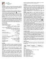
Страница 23: ...ck RF level of COBBA_D pin no 10 P 13 dBm Check UHF Vcnt TP31 V 2 0 2 5 V Start synthesizer troubleshooting TDMA800 RX chain OK Y N N Y N Start synthesizer troubleshooting Change EXT RF Connector Note Check all soldering and components in antenna circuit before changing N Y Y Change duplex filter or L701 Note Check all soldering and discrete components of frontend Change N701 Y Note AG2 is on TP11...

Страница 24: ...also AGC1 line TP10LU Check COBBA_D IF2D N250 pin 9 10 P 13 dBm Change capacitors C790 R789 Check input of IF amplifier P 40 dBm Change Z741 Note Check all components around of filter Measure IF amplifier biasvoltage should be about x x V if not change V741 TP8LU N Y N Y N Y N Change N701 Note Check MXR IF level F 116 19 MHz P 42 dBm N pin 14 Start synthesizer N troubleshooting Check input level o...

Страница 25: ... RF level of COBBA_D pin no 10 P 13 dBm Check UHF Vcnt TP5U V 2 0 2 5V Start synthesizer troubleshooting TDMA1900 RX chain is OK Y N N Y N Start synthesizer troubleshooting Change EXT RF Connector Note Check all soldering and components in antenna circuit before changing N Y Y Change duplex filter or L721 Note Check all soldering and discrete components of frontend Change N721 Y Note AG2 is on Che...

Страница 26: ... COBBA_D IF2D P 13 dBm Change capacitors C790 R789 Check input of IF amplifier P 35 dBm Change Z741 Note Check all components around of filter Measure IF amplifier biasvoltage should be about 1 3 V if not change V741 N Y N Y N Y N Check MXR IF level F 116 19 MHz P 38 dBm Change N721 Note N Y Change N721 Start synthesizer troubleshooting Check input level fo front end N721 pin 1 f 2076 21 MHz V741 ...

Страница 27: ...t be taken from its vacuum package and the heating process must be done in less than 30 second Note that the bottom plate of the chip must be properly soldered and excessive solder material if any has to be remove If any components in the TX chain are replaced the power level tunings have to be checked and retuned Path of the transmitted signal Block level listing AMPS DAMPS Block level listing TD...

Страница 28: ...d input power Should be 10 dBm and f 997 68 MHz If not start synth trouble shooting tx local are missing Replace PA Check VAPC V 2 2V Y N Check PA input PWR P 0 dBm Change PA Y Y N N Check Band passfilter insertion loss max 4dB Check Z901 R907 and C929 Y N Check TXC V 1 5 V Y Start Power control troubleshooting N Change N902 Is TX driver input OK P 20 dBm Y N check for eventual delamination Check ...

Страница 29: ...9 Check TXIF Z900 Pin7 f 161 19 MHz P 25 dBm Change N900 Is Z900 Insertion too high I L 5 dB Change Z900 Check modulator output N750 pin62 P max 18dBm Check R906 Is TX I Q OK V 0 8 VDC 0 4 V symmetrical Change N750 Y N Y N N Y N Y Note check also I Q resistors upconverter Check COBBA I Q DACs baseband ...

Страница 30: ...the same as in AMPS mode but the power amplifier is biased to more linear Consequently it is essential that the AMPS is free of any faults Is AMPS mode OK Start AMPS troubleshooting Check Vbias PIN16 N903 V 2 7 V Start modulator output tuning Is one gain step 2 dB in the output power Change N750 N Y N Y N Check CCONT VR7_bias baseband and or COBBA ...

Страница 31: ...y faults Is TDMA800 mode OK Start TDMA800 troubleshooting Are LO signals OK Start synth troubleshooting Check current consumption I 450mArms Check antenna circuit and Duplex filter N Y N Y Y Note Check VHF and UHF locals including Lo buffer measuring point for UHF is N980 pin5 Make press down test for PA Inreasing current consumption Y N N Short circuit in PA Resolder or change PA Note The PA grou...

Страница 32: ...1 5V PL2 Change PA Y Y N Start power control troubleshooting Check Z951 filter insertion loss Max 4 dB Change BPF Change N950 Check COBBA TXCDAC BaseBand Check TX driver input P 20 dBm Y N N Y N Y N Check N980 upconverter output P 20dBm Check Z950 insertion loss Check TX IF P 25 dBm f 196 23 MHz Check Z900 Insertion loss if less than 4 dB change N750 Y N N Max 4 dB ...

Страница 33: ...ar N750 Press N750 Change N750 Note See DETO vs Output power Note 1 Gain control voltage of driver is directly proportional to output power and TXC voltage in AMPS MODE 2 Gain coltrol voltage of driver will remain same 2dB typ regardless of power level and TXC voltage in DIGITAL MODE 3 DETO and TXC will be about same in each mode 4 TXA is high during modulation 5 TXLX signals will draw about 4mA c...

Страница 34: ...he Integrator capacitor If the voltage is stable and reasonable the local oscillators are running correctly 19 44 MHz reference oscillator The 19 44 MHz oscillator frequency G850 is controlled by the COBBA_D This signal is fed to the PLUSSA and TDMA1900 PLL circuit All synthesiz ers use the divided signal as reference signal for the phase locked loop to provide a correct LO frequency The VCTCXO ou...

Страница 35: ...fer Check also coil L850 capacitor C858 Check resistor R850 Check 2G PLL N880 pin 15 V 0 3 Vpp Change capacitor C851 Check RFC buffer output C857 Change capacitor C853 Note Check all solderings and components of buffer Check 3X output V 150 mVpp Change capacitor C854 Note Check all soldering and components of multiplier Check also Vce should be 1 V if not change V840 N Y Start COBBA_D troubleshoot...

Страница 36: ... two frequencies it also has two diferent switching modes These modes are controlled by the BAND signal In AMPS and TDMA800 modes the frequency is 322 38 MHz and the logical level of the BAND signal is HIGH In TDMA1900 mode a higher if is needed and the operating frequency is increased to 392 46 MHz The BAND signal is also set to logical level zero The VHF VCOoutput signal is fed to the PLUSSA LO ...

Страница 37: ...llator output level P 20 dBm Check V800 Vce pin2 V 2 0 2 5V Note Check BAND signal status 1 TDMA800 AMPS 0 TDMA1900 Note SENA1 PLUSSA PLL SENA2 2G PLL N880 pin 13 Y N Check V800 Vce pin5 Y Y N Change V800 Note Check all solderings and missing components Check D801 V opposite of BAND Change D801 Note Check all components and soldering Start BB troubleshooting PLUSSA pin 8 V 2 0 2 5V N pin 4 Check P...

Страница 38: ...oting Is Frequency locked N What is VCO output level G820 P 0 dBm Check local input level of frontend N701 pin 1 P 0 dBm Change G820 Check R821 Check feedback input level of PLUSSA N750 pin 21 P 10 dBm Check C821 Note Frequency 985 23 1010 2 Vcnt 1 2 3 6 V Note Check all soldering missing components N Y N Y N N Check PLUSSA N750 pin 54 SCLK 2 8V pin 55 SDATA 2 8V pin 56 SENA1 2 8V SENA is 0 during...

Страница 39: ...ircuit 2 GHz UHF synthesizer troubleshooting Is Frequency locked N What is VCO output level G860 P 0 dBm Check local input level of frontend N721 pin 1 P 0 dBm Change G860 Check R867 Check feedback input level of N880 pin 6 P 10 dBm Check R886 Note Frequency 985 23 1010 2 Vcnt 1 2 3 6 V C861 Note Check all soldering missing components N Y N Y N N Check N880 pin 11 SCLK 2 8V pin 12 SDATA 2 8V pin 1...

Страница 40: ...ÁÁÁÁÁÁ ÁÁÁÁÁÁÁÁÁÁÁÁÁÁÁÁÁÁÁÁ Positive supply voltage for the 1st opamp in pwrcnrl ÁÁÁÁ ÁÁÁÁ 11 ÁÁÁÁÁÁ ÁÁÁÁÁÁ TXC_pwc ÁÁÁÁ ÁÁÁÁ 0 5 2VÁÁÁÁÁÁÁÁÁÁÁÁÁÁÁÁÁÁÁÁ ÁÁÁÁÁÁÁÁÁÁÁÁÁÁÁÁÁÁÁÁ Power level control of the TX ÁÁÁÁ ÁÁÁÁ 12 ÁÁÁÁÁÁ ÁÁÁÁÁÁ DET_pwc ÁÁÁÁ ÁÁÁÁ ÁÁÁÁÁÁÁÁÁÁÁÁÁÁÁÁÁÁÁÁ ÁÁÁÁÁÁÁÁÁÁÁÁÁÁÁÁÁÁÁÁ Feedback from the peak detector diode ÁÁÁÁ ÁÁÁÁ 13 ÁÁÁÁÁÁ ÁÁÁÁÁÁ TXI_pwc ÁÁÁÁ ÁÁÁÁ ÁÁÁÁÁÁÁÁÁÁÁÁÁÁÁÁÁÁÁÁ ÁÁÁÁÁ...

Страница 41: ...e output of analog mode RX mixer ÁÁÁÁ ÁÁÁÁ 46 ÁÁÁÁÁÁ ÁÁÁÁÁÁ UB_a1 ÁÁÁÁ ÁÁÁÁ ÁÁÁÁÁÁÁÁÁÁÁÁÁÁÁÁÁÁÁÁ ÁÁÁÁÁÁÁÁÁÁÁÁÁÁÁÁÁÁÁÁ Filtering cap for bias of analog mode RX ÁÁÁÁ ÁÁÁÁ 47 ÁÁÁÁÁÁ ÁÁÁÁÁÁ VRX ÁÁÁÁ ÁÁÁÁ 2 8V ÁÁÁÁÁÁÁÁÁÁÁÁÁÁÁÁÁÁÁÁ ÁÁÁÁÁÁÁÁÁÁÁÁÁÁÁÁÁÁÁÁ Power supply of the receiver ÁÁÁÁ ÁÁÁÁ 48 ÁÁÁÁÁÁ ÁÁÁÁÁÁ GND_if1 ÁÁÁÁ ÁÁÁÁ 0 ÁÁÁÁÁÁÁÁÁÁÁÁÁÁÁÁÁÁÁÁ ÁÁÁÁÁÁÁÁÁÁÁÁÁÁÁÁÁÁÁÁ Ground ÁÁÁÁ ÁÁÁÁ 49 ÁÁÁÁÁÁ ÁÁÁÁÁÁ I...

Страница 42: ...ÁÁÁÁ Pin nameÁÁÁÁ ÁÁÁÁ ÁÁÁÁ ÁÁÁÁ Nomi nal lev el ÁÁÁÁÁÁÁÁÁÁÁÁÁÁÁÁÁÁÁ ÁÁÁÁÁÁÁÁÁÁÁÁÁÁÁÁÁÁÁ ÁÁÁÁÁÁÁÁÁÁÁÁÁÁÁÁÁÁÁ ÁÁÁÁÁÁÁÁÁÁÁÁÁÁÁÁÁÁÁ Description N960 ÁÁÁÁ ÁÁÁÁ 1 ÁÁÁÁÁ ÁÁÁÁÁ Vcc ÁÁÁÁ ÁÁÁÁ VBATÁÁÁÁÁÁÁÁÁÁÁÁÁÁÁÁÁÁÁ ÁÁÁÁÁÁÁÁÁÁÁÁÁÁÁÁÁÁÁ Power supply for bias circuit ÁÁÁÁ ÁÁÁÁ 2 ÁÁÁÁÁ ÁÁÁÁÁ N C ÁÁÁÁ ÁÁÁÁ ÁÁÁÁÁÁÁÁÁÁÁÁÁÁÁÁÁÁÁ ÁÁÁÁÁÁÁÁÁÁÁÁÁÁÁÁÁÁÁ Not connected ÁÁÁÁ ÁÁÁÁ 3 ÁÁÁÁÁ ÁÁÁÁÁ LTune ÁÁÁÁ ÁÁÁÁ ÁÁÁÁÁÁÁÁÁÁ...

Страница 43: ...e ÁÁÁÁÁ ÁÁÁÁÁ ÁÁÁÁÁ ÁÁÁÁÁ Ground ÁÁÁÁ ÁÁÁÁ ÁÁÁÁ ÁÁÁÁ ÁÁÁÁÁÁÁÁÁÁÁÁÁÁÁÁÁÁÁ ÁÁÁÁÁÁÁÁÁÁÁÁÁÁÁÁÁÁÁ ÁÁÁÁÁÁÁÁÁÁÁÁÁÁÁÁÁÁÁ ÁÁÁÁÁÁÁÁÁÁÁÁÁÁÁÁÁÁÁ Ground connection The backside of the pack age must be connected to the ground plane throught a short path PENTA regulator ÁÁÁÁ ÁÁÁÁ ÁÁÁÁ ÁÁÁÁ Pin ÁÁÁÁÁ ÁÁÁÁÁ ÁÁÁÁÁ ÁÁÁÁÁ Pin nameÁÁÁÁ ÁÁÁÁ ÁÁÁÁ ÁÁÁÁ Nomi nal lev el ÁÁÁÁÁÁÁÁÁÁÁÁÁÁÁÁÁÁÁ ÁÁÁÁÁÁÁÁÁÁÁÁÁÁÁÁÁÁÁ ÁÁÁÁÁÁÁÁÁÁÁÁ...

Страница 44: ...ÁÁÁÁÁÁÁÁÁÁÁ ÁÁÁÁÁÁÁÁÁÁÁÁÁÁÁÁÁÁÁ ÁÁÁÁÁÁÁÁÁÁÁÁÁÁÁÁÁÁÁ Description ÁÁÁÁ ÁÁÁÁ 1 ÁÁÁÁÁ ÁÁÁÁÁ FAST ÁÁÁÁ ÁÁÁÁ 2 8VÁÁÁÁÁÁÁÁÁÁÁÁÁÁÁÁÁÁÁ ÁÁÁÁÁÁÁÁÁÁÁÁÁÁÁÁÁÁÁ Enable input for fast chargepump ÁÁÁÁ ÁÁÁÁ 2 ÁÁÁÁÁ ÁÁÁÁÁ CPF ÁÁÁÁ ÁÁÁÁ ÁÁÁÁÁÁÁÁÁÁÁÁÁÁÁÁÁÁÁ ÁÁÁÁÁÁÁÁÁÁÁÁÁÁÁÁÁÁÁ Fast charge pump output ÁÁÁÁ ÁÁÁÁ 3 ÁÁÁÁÁ ÁÁÁÁÁ CP ÁÁÁÁ ÁÁÁÁ ÁÁÁÁÁÁÁÁÁÁÁÁÁÁÁÁÁÁÁ ÁÁÁÁÁÁÁÁÁÁÁÁÁÁÁÁÁÁÁ Normal charge pump output ÁÁÁÁ ÁÁÁÁ 4 ÁÁÁ...

Отзывы: