1-10
|
ni.com
Chapter 1
Getting Started
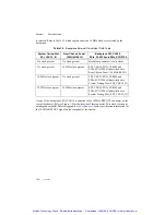
is selected. Refer to Table 1-2 which explains how the 10 MHz clocks are selected by the
backplane.
A copy of the backplane’s PXI_CLK10 is exported to the 10 MHz REF OUT connector on the
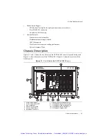
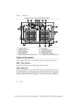
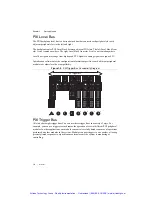
rear of the chassis. Refer to Figure 1-2 for the location of this connector. This clock is driven by
an independent buffer. Refer to Appendix A,
Specifications
, for the specification information for
the 10 MHz REF OUT signal on the rear panel of the chassis.
Table 1-2.
Backplane External Clock Input Truth Table
System Timing Slot
PXI_CLK10_IN
Rear Chassis Panel
10 MHz REF IN
Backplane PXI_CLK10,
PXIe_CLK100 and PXIe_SYNC100
No clock present
No clock present
Backplane generates its own clocks
No clock present
10 MHz clock present
PXI_CLK10, PXIe_CLK100 and
PXIe_SYNC100 all phase-locked to
Rear Chassis Panel—10 MHz REF IN
10 MHz clock present
No clock present
PXI_CLK10, PXIe_CLK100 and
PXIe_SYNC100 all phase-locked to
System Timing Slot—PXI_CLK10_IN
10 MHz clock present
10 MHz clock present
PXI_CLK10, PXIe_CLK100 and
PXIe_SYNC100 all phase-locked to
System Timing Slot—PXI_CLK10_IN
Artisan Technology Group - Quality Instrumentation ... Guaranteed | (888) 88-SOURCE | www.artisantg.com

