591
Chapter 14
A/D Converter
User’s Manual U16580EE3V1UD00
14.5 Operation in A/D Trigger Mode
When the ADCEn bit of the ADMn0 register is set to 1, A/D conversion is started.
14.5.1 Select mode operation
In this mode, the analog input specified by the ADMn2 register is A/D converted. The conversion results
are stored in the ADCRnm register corresponding to the analog input. In the select mode, the 1-buffer
mode and 4-buffer mode are supported according to the storing method of the A/D conversion results
(n = 0, 1), (m = 0 to 9).
(1)
1-buffer mode (A/D trigger select: 1 buffer)
In this mode, one analog input is A/D converted once. The conversion results are stored in one
ADCRn register. The analog input and ADCRn register correspond one to one.
Each time an A/D conversion is executed, an A/D conversion end interrupt (INTAD) is generated
and A/D conversion ends. The next conversion operation is repeated, unless the ADCE bit of the
ADM0 register is cleared to 0.
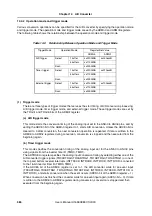
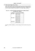
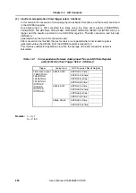
Table 14-3:
Correspondence Between Analog Input Pins and ADCRnm Register
(A/D Trigger Select: 1 Buffer)
This mode is most appropriate for applications in which the results of each first-time A/D conver-
sion are read.
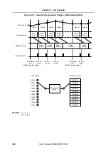
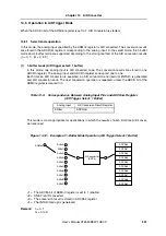
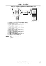
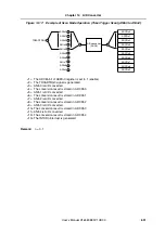
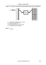
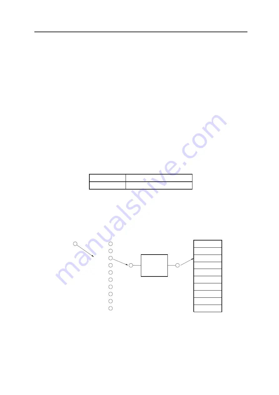
Figure 14-12:
Example of 1-Buffer Mode Operation (A/D Trigger Select: 1 Buffer)
<1> The ADCEn bit of ADMn0 register is set to 1 (enable)
<2> ANIn2 is A/D converted
<3> The conversion result is stored in ADCRn2 register
<4> The INTAD interrupt is generated
Remark:
n = 0, 1
m = 0 to 9
Analog Input
A/D Conversion Result Register
ANInm
ADCRnm
ANIn0
ANIn1
ANIn2
ANIn3
ANIn4
ANIn5
ANIn6
ANIn7
ANIn8
ANIn9
ADCRn0
ADCRn1
ADCRn2
ADCRn3
ADCRn4
ADCRn5
ADCRn6
ADCRn7
ADCRn8
ADCRn9
A/D converter
(ADCn)
ADMn2
Содержание V850E/PH2
Страница 6: ...6 Preface User s Manual U16580EE3V1UD00...
Страница 16: ...16 User s Manual U16580EE3V1UD00...
Страница 28: ...28 User s Manual U16580EE3V1UD00...
Страница 32: ...32 User s Manual U16580EE3V1UD00...
Страница 84: ...84 Chapter 2 Pin Functions User s Manual U16580EE3V1UD00 MEMO...
Страница 144: ...144 Chapter 3 CPU Functions User s Manual U16580EE3V1UD00 MEMO...
Страница 192: ...192 Chapter 5 Memory Access Control Function PD70F3187 only User s Manual U16580EE3V1UD00 MEMO...
Страница 312: ...312 Chapter 9 16 Bit Timer Event Counter P User s Manual U16580EE3V1UD00 MEMO...
Страница 534: ...534 Chapter 11 16 bit Timer Event Counter T User s Manual U16580EE3V1UD00...
Страница 969: ...969 Chapter 20 Port Functions User s Manual U16580EE3V1UD00 MEMO...
Страница 970: ...970 Chapter 20 Port Functions User s Manual U16580EE3V1UD00...
Страница 976: ...976 Chapter 22 Internal RAM Parity Check Function User s Manual U16580EE3V1UD00 MEMO...
Страница 984: ...984 Chapter 23 On Chip Debug Function OCD User s Manual U16580EE3V1UD00 MEMO...
Страница 1006: ...1006 Chapter 24 Flash Memory User s Manual U16580EE3V1UD00 MEMO...
Страница 1036: ...1036 Chapter 27 Recommended Soldering Conditions User s Manual U16580EE3V1UD00 MEMO...
Страница 1046: ...1046 Appendix A Index User s Manual U16580EE3V1UD00 MEMO...
Страница 1052: ...1052 User s Manual U16580EE3V1UD00...
Страница 1053: ......


