background image

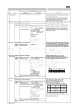
Temperature

Compensating Type

High Dielectric
Constant Type

16

Humidity

Appearance

No defects or abnormalities.

Set the capacitor at 40±2

 and in 90 to 95% humiduty

(Steady State)

for 500±12 hours.

Capacitance

Within 

±

5% or

±

 0.5pF

B1,B3,R1,R6,R7,R9,C7,C8,L8:Within 

±

12.5%

Remove and set for 24±2 hours at room temperature, 

Change

(Whichever is larger)

F1,F5      :Within 

±

30%

then measure.

Q/D.F.

30pF and over:Q

350

B1,B3,R1,R6,R7,C7,C8,L8

10pF and over

W.V.:100V :0.05max.( C

0.068

m

F)

30pF and below:Q

275+5C/2

                  :0.075max.(C

0.068

m

F)

10pF and below:Q

200+10C

W.V.:50V/25V :0.05max.
W.V.:16V/10V :0.05max.

 C:Nominal Capacitance(pF)

W.V.:6.3V/4V  :0.075max.(C

3.3

m

F)

                       :0.125max.(C

3.3

m

F)

[R9]
W.V.:50V: 0.075max.
[F1,F5]
W.V.:25Vmin

    :0.075max. (C

0.1

m

F)

    :0.125max. (C

0.1

m

F)

W.V.:16V/10V:0.15max.

W.V.:6.3V:0.2max.

I.R.

More than 1,000M

W

 or 50

W

·F(Whichever is smaller)

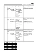
17

Humidity Load

Appearance

No defects or abnormalities.

Apply the rated voltage at 40±2

 and 90 to 95% humidity

for 500±12 hours. Remove and set for 24±2 hours at room 

Capacitance Within 

±

7.5% or

±

0.75pF

B1,B3,R1,R6,R7,R9,C7,C8,L8:

Within


±

12.5%

temprature, then muasure. The charge/discharge current 

Change

(Whichever is larger)

F1,F5      :Within 

±

30%

is less than 50mA.

[W.V.:10Vmax.]

F1  :30/-40%

Q/D.F.

30pF and over:Q

200

B1,B3,R1,R6,R7,C7,C8,L8

• Initial measurement for F1/10Vmax.

30pF and below:Q

100+10C/3 W.V.:100V :0.05max.( C

0.068

m

F)

Apply the rated DC voltage for 1 hour at 40±2

.

                  :0.075max.(C

0.068

m

F)

Remove and set for 24±2 hours at room temperature.

   C:Nominal Capacitance(pF)

W.V.:50V/25V :0.05max.

Perform initial measurement.

W.V.:16V/10V :0.05max.

W.V.:6.3V/4V  :0.075max.(C

3.3

m

F)

                       :0.125max.(C

3.3

m

F)


[R9]
W.V.:50V: 0.075max.
[F1,F5]
W.V.:25Vmin

    :0.075max. (C

0.1

m

F)

    :0.125max. (C

0.1

m

F)

W.V.:16V/10V:0.15max.

W.V.:6.3V:0.2max.

I.R.

More than 500MΩ or 25Ω·F(Whichever is smaller)

18

High Temperature

Appearance No defects or abnormalities.

Apply 200% of the rated voltage at the maximum

Load

operating temperature±3

 for 1000±12 hours.

Capacitance

Within 

±

3% or 

±

0.3pF

B1,B3,R1,R6,R7,R9,C7,C8,L8:

Within


±

12.5%

Set for 24±2 hours at room temperature, then measure.

Change

(Whichever is larger)

F1,F5      :Within 

±

30%

The charge/discharge current is less than 50mA.

[Except 35V,10Vmax and C

1.0. 

m

F]


F1  :30/-40%

[35V, 10Vmax and C

1.0. 

m

F]

Q/D.F.

30pF and over:Q

350

B1,B3,R1,R6,R7,C7,C8,L8

Initial measurement for high dielectric constant type.

10pF and over

W.V.:100V :0.05max.( C

0.068

m

F)

 Apply 200% of the rated DC voltage at the maximun operating

30pF and below: Q

275+5C/2

                  :0.075max.(C

0.068

m

F)

 temperature ±3°C for one hour. Remove and set for

10pF and below:Q

200+10C

W.V.:50V/25V  :0.05max.

 24±2 hours at room temperature.

W.V.:16V/10V  :0.05max.

 Perform initial measurement.

   C:Nominal Capacitance (pF)

W.V.:6.3V/4V   :0.075max.(C

3.3

m

F)

                        :0.125max.(C

3.3

m

F)

[R9]
W.V.:50V: 0.075max.
[F1,F5]
W.V.:25Vmin

    :0.075max. (C

0.1

m

F)

    :0.125max. (C

0.1

m

F)

W.V.:16V/10V:0.15max.

W.V.:6.3V:0.2max.

I.R.

More than 1,000M

W

 or 50

W

·F(Whichever is smaller)

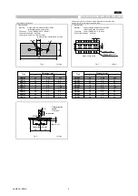
SPECIFICATIONS AND TEST METHODS

No

Item

Specification

Test Method

Table A


Char. 

Nominal 

Values 

(ppm/

C) * 

Capacitance Change from 20

C (%) 

-55 

-25 

-10 

Max. 

Min. 

Max. 

Min. 

Max. 

Min. 

2C/0C 

      0

±

  60 

0.82 

-0.45 

0.49 

-0.27 

0.33 

-0.18 

3C 

      0

±

120 

1.37 

-0.90 

0.82 

-0.54 

0.55 

-0.36 

4C 

      0

±

250 

2.56 

-1.88 

1.54 

-1.13 

1.02 

-0.75 

2P 

-150

±

  60 

1.32 

  0.41 

0.88 

  0.27 

3P 

-150

±

120 

1.65 

  0.14 

1.10 

  0.09 

4P 

-150

±

250 

2.36 

-0.45 

1.57 

-0.30 

2R 

-220

±

  60 

1.70 

  0.72 

1.13 

  0.48 

3R 

-220

±

120 

2.03 

  0.45 

1.35 

  0.30 

4R 

-220

±

250 

2.74 

-0.14 

1.83 

-0.09 

2S 

-330

±

  60 

2.30 

  1.22 

1.54 

  0.81 

3S 

-330

±

120 

2.63 

  0.95 

1.76 

  0.63 

4S 

-330

±

250 

3.35 

  0.36 

2.23 

  0.24 

2T 

-470

±

  60 

3.07 

  1.85 

2.05 

  1.23 

3T 

-470

±

120 

3.40 

  1.58 

2.27 

  1.05 

4T 

-470

±

250 

4.12 

  0.99 

2.74 

  0.66 

3U 

-750

±

120 

4.94 

  2.84 

3.29 

  1.89 

4U 

-750+250 

5.65 

  2.25 

3.77 

  1.50 

1X 

+350 to -1000 

* Nominal values denote the temperature coefficient within a range of 20

C to 125

C(for 

C)/ 150

C(for 0C)/85

C(for other TC).


JEMCGS-0001S

4

Содержание GRM21BE71C475MA12K

Страница 1: ... 20 30 to 85 C 82 to 22 30 to 85 C 25 C 3 Temperature Characteristics Public STD Code Y5V EIA Specifications and Test Methods Operationg Temp Range Temp coeff or Cap Change 5 Nominal Capacitance 6 Capacitance Tolerance 25 Vdc 0 7 min 2 T 1 25 0 1 This product specification is applied to Chip Monolithic Ceramic Capacitor used for General Electronic equipment 1 1 L 2 0 0 1 1 2 W 1 25 0 1 e L f180mm ...

Страница 2: ...at each Temperature tolerance Table A 25 C to 85 C specified temp stage Characteristics R1 R7 Within 15 1 Temperature Compensating Type 55 C to 125 C The temperature coefficient is determind using the capacitance R6 Within 15 measured in step 3 as a reference 55 C to 85 C When cycling the temperature sequentially from step 1 through R9 Within 15 5 Δ C 20 to 125 other temp coeffs 20 to 85 the 55 C ...

Страница 3: ...5 seconds at 230 5 or Sn 3 0Ag 0 5Cu solder solution for 2 0 5 seconds at 245 5 14 Resistance to Appearance No defects or abnormalities Preheat the capacitor at 120 to 150 for 1 minute Soldering Heat Immerse the capacitor in an eutectic solder solution or Capacitance Within 2 5 or 0 25pF B1 B3 R1 R6 R7 R9 C7 C8 L8 Within 7 5 Sn 3 0Ag 0 5Cu solder solution at 270 5 for 10 0 5 seconds Change Whichev...

Страница 4: ...Temperature Appearance No defects or abnormalities Apply 200 of the rated voltage at the maximum Load operating temperature 3 for 1000 12 hours Capacitance Within 3 or 0 3pF B1 B3 R1 R6 R7 R9 C7 C8 L8 Within 12 5 Set for 24 2 hours at room temperature then measure Change Whichever is larger F1 F5 Within 30 The charge discharge current is less than 50mA Except 35V 10Vmax and C 1 0 mF F1 Within 30 4...

Страница 5: ...g 1 in mm Fig 3 in mm Fig 2 in mm SPECIFICATIONS AND TEST METHODS Type Dimension mm a b c GRM02 0 2 0 56 0 23 GRM03 0 3 0 9 0 3 GRM15 0 4 1 5 0 5 GRM18 1 0 3 0 1 2 GRM21 1 2 4 0 1 65 GRM31 2 2 5 0 2 0 GRM32 2 2 5 0 2 9 GRM43 3 5 7 0 3 7 GRM55 4 5 8 0 5 6 2 4 0 0 1 8 0 0 3 3 5 0 05 0 05以下 1 φ1 5 0 1 0 A t 1 2 2 0 0 05 1 75 0 1 B 100 40 a c b Land f4 5 c a c b ランド f4 5 c Glass epoxy board Solder re...

Страница 6: ...GR 18 4000 10000 5 6 9 4000 3000 10000 A B 3000 10000 6 9 4000 10000 M X 3000 10000 C 2000 6000 5 6 9 4000 10000 A M 3000 10000 N 2000 8000 C 2000 6000 R D E 1000 4000 M 1000 5000 N C R D 1000 4000 E 500 2000 S 500 1500 M 1000 5000 N C R D 1000 4000 E 500 F X 300 1500 1 2 Dimensions of Tape 1 GR 02 W4P1 CODE L in mm Code GR 02 A 3 0 23 B 3 0 43 3 Nominal value t 0 5 max Package GRM F Type Type GR ...

Страница 7: ...lerance 0 05 GR 15 Dimensions Tolerance 0 05 GR 15 Dimensions Tolerance 0 1 GR 15 Dimensions Tolerance 0 15 GR 15 Dimensions Tolerance 0 2 A 3 0 37 0 39 0 65 0 70 0 72 0 75 B 3 0 67 0 69 1 15 1 20 1 25 1 35 t 0 5max 0 5 max 0 8 max 0 8 max 0 8 max 0 8 max 3 Nominal value 1 0 0 05 4 0 0 1 φ1 5 0 1 0 1 75 0 1 8 0 0 3 3 5 0 05 A B t 1 0 0 05 Code GRM03 GRM15 A 0 37 0 65 B 0 67 1 15 t 0 5max 0 8max No...

Страница 8: ...A 1 05 0 1 1 10 0 1 1 05 0 1 1 55 0 15 2 0 0 2 2 8 0 2 B 1 85 0 1 2 00 0 1 2 00 0 1 2 3 0 15 3 6 0 2 3 6 0 2 8 0 0 3 4 0 0 1 3 5 0 05 1 75 0 1 A B 2 0 0 1 φ1 5 0 1 0 1 7 max T 1 25mm 2 5 max T 1 35 1 6mm 3 0 max T 1 8 2 0mm 3 7 max T 2 5mm 4 0 0 1 0 25 0 1 T 2 0mm 0 3 0 1 T 2 5mm Code GR 21 Dimensions Tolerance 0 1 GR 21 Dimensions Tolerance 0 15 0 2 GR 31 Dimensions Tolerance 0 2 within GR 31 Dim...

Страница 9: ...GR 43 GR 55 A 2 3 6 5 2 B 2 4 9 6 1 2 Nominal value Package GRM F Type φ1 5 0 1 0 4 0 0 1 8 0 0 1 φ1 5 0 2 0 12 0 0 3 5 5 0 1 1 75 0 1 A 1 2 5 max T 1 8mm 3 7 max T 2 0 2 5mm 4 7 max T 2 8mm B 1 2 0 0 1 0 3 0 1 JEMCGP 01796 9 ...

Страница 10: ... specified in 1 2 Base Tape As specified in 1 2 Bottom Tape Thickness 0 05 Only a bottom tape existence W w1 GR 02 8 0 max 5 1 5 GR 32 max 16 5 max 10 1 5 GR 43 55 20 5 max 14 1 5 φ180 0 3 0 φ330 2 0 φ50 min φ13 0 5 2 0 0 5 Chip in mm Fig 1 Package Chips Fig 2 Dimensions of Reel Fig 3 Taping Diagram JEMCGP 01796 10 ...

Страница 11: ... fuzz in the cavity 1 10 Break down force of top tape 5N min Break down force of bottom tape 5N min Only a bottom tape existence 1 11 Reel is made by resin and appeaser and dimension is shown in Fig 2 There are possibly to change the material and dimension due to some impairment 1 12 Peeling off force 0 1N to 0 6N in the direction as shown below GR 02 03 0 05N 0 5N 1 13 Label that show the custome...

Страница 12: ...ight dust rapid temperature changes corrosive gas atmosphere or high temperature and humidity conditions during storage may affect the solderability and the packaging performance Please use product within six months of receipt 2 Please confirm solderability before using after six months Store the capacitors without opening the original bag Even if the storage period is short do not exceed the spec...

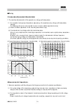
Страница 13: ...ntended environment and operating conditions Typical temperature characteristics Char R6 X5R Typical temperature characteristics Char R7 X7R Typical temperature characteristics Char F5 Y5V 2 Measurement of Capacitance 1 Measure capacitance with the voltage and the frequency specified in the product specifications 1 1 The output voltage of the measuring equipment may decrease when capacitance is hi...

Страница 14: ... Pulse voltage E Maximum possible applied voltage 1 2 Influence of overvoltage Overvoltage that is applied to the capacitor may result in an electrical short circuit caused by the breakdown of the internal dielectric layers The time duration until breakdown depends on the applied voltage and the ambient temperature 4 Applied Voltage and Self heating Temperature 1 When the capacitor is used in a hi...

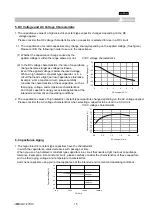
Страница 15: ...ture characteristics And check capacitors using your actual appliances at the intended environment and operating conditions 2 The capacitance values of high dielectric constant type capacitors change depending on the AC voltage applied Please consider the AC voltage characteristics when selecting a capacitor to be used in a AC circuit AC voltage characteristics 6 Capacitance Aging 1 The high diele...

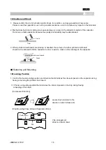
Страница 16: ...nted circuit board should not be allowed to hit the capacitor in order to avoid a crack or other damage to the capacitor Soldering and Mounting 1 Mounting Position 1 Confirm the best mounting position and direction that minimizes the stress imposed on the capacitor during flexing or bending the printed circuit board 1 1 Choose a mounting position that minimizes the stress imposed on the chip durin...

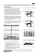
Страница 17: ...essive forces are not applied to the capacitors 1 1 In mounting the capacitors on the printed circuit board any bending force against them shall be kept to a minimum to prevent them from any bending damage or cracking Please take into account the following precautions and recommendations for use in your process 1 Adjust the lowest position of the pickup nozzle so as not to bend the printed circuit...

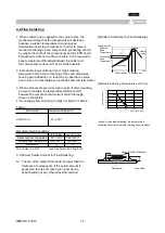
Страница 18: ...ions Infrared Reflow Vapor Reflow Peak Temperature 230 250 230 240 240 260 Atmosphere Air Air Air or N2 Pb Sn Solder Sn 37Pb Lead Free Solder Sn 3 0Ag 0 5Cu In case of repeated soldering the accumulated soldering time must be within the range shown above 4 Optimum Solder Amount for Reflow Soldering 4 1 Overly thick application of solder paste results in a excessive solder fillet height This makes ...

Страница 19: ...maintain the temperature difference ΔT between the component and solvent within the range shown in the table 2 4 Do not apply flow soldering to chips not listed in Table 2 Table 2 Temperature Differential In case of repeated soldering the accumulated soldering time must be within the range shown above Recommended Conditions Pb Sn Solder Lead Free Solder 90 110 100 120 240 250 250 260 Air N2 Pb Sn ...

Страница 20: ...Lead Free Solder Sn 3 0Ag 0 5Cu 4 Optimum Solder amount when re working with a Soldering lron 4 1 In case of sizes smaller than 0603 GR 03 15 18 the top of the solder fillet should be lower than 2 3 s of the thickness of the component or 0 5mm whichever is smaller In case of 0805 and larger sizes GR 21 31 32 43 55 the top of the solder fillet should be lower in section than 2 3 s of the thickness ...

Страница 21: ...ormance of a capacitor after mounting on the printed circuit board 1 1 Avoid bending printed circuit board by the pressure of a test pin etc The thrusting force of the test probe can flex the PCB resulting in cracked chips or open solder joints Provide support pins on the back side of the PCB to prevent warping or flexing 1 2 Avoid vibration of the board by shock when a test pin contacts a printed...

Страница 22: ...g and from the front side of board as below the capacitor may form a crack caused by the tensile stress applied to capacitor Outline of jig 2 Example of a suitable machine An outline of a printed circuit board cropping machine is shown as follows Along the lines with the V grooves on printed circuit board the top and bottom blades are aligned to one another when cropping the board The misalignment...

Страница 23: ...t can cause condensation 2 Others 2 1 In an Emergency 1 If the equipment should generate smoke fire or smell immediately turn off or unplug the equipment If the equipment is not turned off or unplugged the hazards may be worsened by supplying continuous power 2 In this type of situation do not allow face and hands to come in contact with the capacitor or burns may be caused by the capacitors high ...

Страница 24: ... capacitors 1 1 The capacitor when used in the above unsuitable operating environments may deteriorate due to the corrosion of the terminations and the penetration of moisture into the capacitor 1 2 The same phenomenon as the above may occur when the electrodes or terminals of the capacitor are subject to moisture condensation 1 3 The deterioration of characteristics and insulation resistance due ...

Страница 25: ...lity of chip crack caused by PCB expansion contraction with heat Because stress for chip is different depend on PCB material and structure Especially metal PCB such as alumina has a greater risk of chip crack because of large difference of thermal expansion coefficient In case of chip below 0402 size there is also the same possibility of crack with a single layered glass epoxy board Pattern Forms ...

Страница 26: ... GR 32 3 2 2 5 2 0 2 4 1 0 1 2 1 8 2 3 GR 43 4 5 3 2 3 0 3 5 1 2 1 4 2 3 3 0 GR 55 5 7 5 0 4 0 4 6 1 4 1 6 3 5 4 8 in mm GR 21 1 9 2 1 1 0 1 3 1 7 1 9 2 0 1 25 0 15 1 2 0 6 0 8 1 2 1 4 GR 31 3 2 1 6 within 0 20 1 8 2 0 0 9 1 2 1 5 1 7 3 2 1 6 0 30 1 2 1 4 2 0 1 25 0 20 0 9 1 0 0 8 1 1 GR 18 2 0 1 25 within 0 10 1 2 0 6 1 25 1 0 1 4 0 6 0 8 c Notice Chip L W a b c 0 8 0 9 0 6 0 8 2 0 1 25 1 0 1 2 G...

Страница 27: ...trol curing temperature and time in order to prevent insufficient hardening 4 Flux Application 1 An excessive amount of flux generates a large quantity of flux gas which can cause a deterioration of Solderability So apply flux thinly and evenly throughout A foaming system is generally used for flow soldering 2 Flux containing too a high percentage of halide may cause corrosion of the outer electro...

Страница 28: ...sed as an under coating to buffer against the stress 2 Select a resin that is less hygroscopic Using hygroscopic resins under high humidity conditions may cause the deterioration of the insulation resistance of a capacitor An epoxy resin can be used as a less hygroscopic resin Others 1 Transportation 1 The performance of a capacitor may be affected by the conditions during transportation 1 1 The c...

Страница 29: ...ication 3 We consider it not appropriate to include any terms and conditions with regard to the business transaction in the product specifications drawings or other technical documents Therefore if your technical documents as above include such terms and conditions such as warranty clause product liability clause or intellectual property infringement liability clause they will be deemed to be inva...

Отзывы: