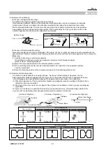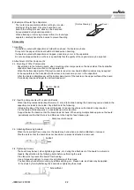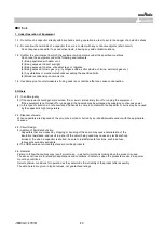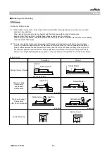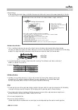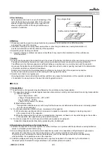
2. Land Dimensions
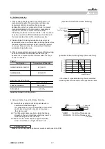
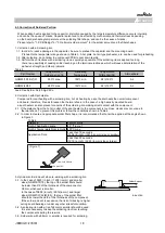
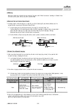
2-1. Chip capacitors can be cracked due to the stress
of PCB bending , etc. if the land area is larger than
needed and has an excess amount of solder.
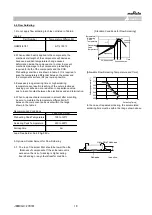
Please refer to the land dimensions in table 1
for flow soldering, table 2 for reflow soldering.
Please confirm the suitable land dimension by
evaluating of the actual SET / PCB.
Table 1 Flow Soldering Method
Dimensions
Part Number
Flow soldering can only be used for products with a chip size of 1.6x0.8mm to 3.2x1.6mm.
(in mm)
Table 2 Reflow Soldering Method
Dimensions
Part Number
1.0×0.5
(within ±0.10)
1.0×0.5
(
±0.15/±0.20
)
1.6×0.8
(within ±0.10)
1.6×0.8
(±0.15/±0.20)
2.0×1.25
(within ±0.10)
2.0×1.25
(±0.15)
2.0×1.25
(±0.20)
3.2×1.6
(within±0.20)
3.2×1.6
(±0.30)
(in mm)
GRM01
0.25×0.125
0.10 to 0.11
0.07 to 0.12
0.125 to 0.145
0.4 to 0.6
0.40 to 0.50
GRM31
3.2×1.6
2.2 to 2.6
1.0 to 1.1
GRM02
0.4×0.2
0.16 to 0.2
0.12 to 0.18
Notice
L×W
a
b
c
0.8 to 0.9
GRM18
0.6 to 0.8
1.6×0.8
0.6 to 1.0
c
2.0×1.25
1.0 to 1.2
GRM21
a
L×W
(Dimensions
Tolerance)
0.9 to 1.0
0.8 to 1.1
1.0 to 1.4
b
0.2 to 0.23
GRM03
0.6×0.3
0.2 to 0.3
0.6
1.25
GRM21
0.6 to 0.8
0.2 to 0.35
0.2 to 0.4
0.6 to 0.8
1.2 to 1.4
0.4 to 0.6
0.5 to 0.7
0.6 to 0.8
0.6 to 0.7
0.6 to 0.8
0.7 to 0.8
0.8 to 1.0
0.35 to 0.45
1.2 to 1.4
2.3 to 3.0
1.2 to 1.4
1.8 to 2.0
0.9 to 1.2
1.5 to 1.7
1.9 to 2.1
1.0 to 1.3
1.7 to 1.9
1.0 to 1.4
1.4 to 1.6
3.5 to 4.8
GRM43
GRM55
GRM32
3.2×2.5
2.0 to 2.4
1.0 to 1.2
1.8 to 2.3
4.5×3.2
GRM31
GRM15
GRM18
5.7×5.0
4.0 to 4.6
3.0 to 3.5
1.2
0.7 to 0.9
0.3 to 0.5
1.2
c
b
a
Solder Resist
Chip Capacitor
Land
JEMCGC-2701W
26


