■
Soldering and Mounting
1.PCB Design
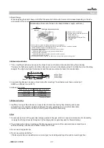
1. Notice for Pattern Forms
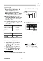
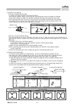
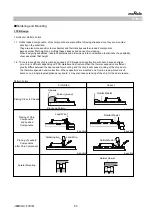
1-1. Unlike leaded components, chip components are susceptible to flexing stresses since they are mounted
directly on the substrate.
They are also more sensitive to mechanical and thermal stresses than leaded components.
Excess solder fillet height can multiply these stresses and cause chip cracking.
When designing substrates, take land patterns and dimensions into consideration to eliminate the possibility
of excess solder fillet height.
1-2. There is a possibility of chip cracking caused by PCB expansion/contraction with heat, because stress
on a chip is different depending on PCB material and structure.When the thermal expansion coefficient
greatly differs between the board used for mounting and the chip,it will cause cracking of the chip due to
the thermal expansion and contraction. When capacitors are mounted on a fluorine resin printed circuit
board or on a single-layered glass epoxy board, it may also cause cracking of the chip for the same reason.
Pattern Forms
in section
in section
in section
in section
in section
in section
Notice
Placing of Leaded
Components
after Chip Component
Lateral Mounting
Prohibited
Correct
Placing Close to Chassis
Placing of Chip
Components
and Leaded
Components
Chassis
Solder (ground)
Electrode Pattern
Solder Resist
Lead Wire
Solder Resist
Lead Wire
Soldering Iron
Solder Resist
ソルダレジスト
Solder Resist
JEMCGC-2701W
25


