


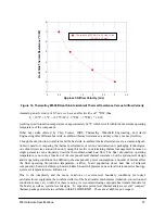
12
603 Hardware Specifications
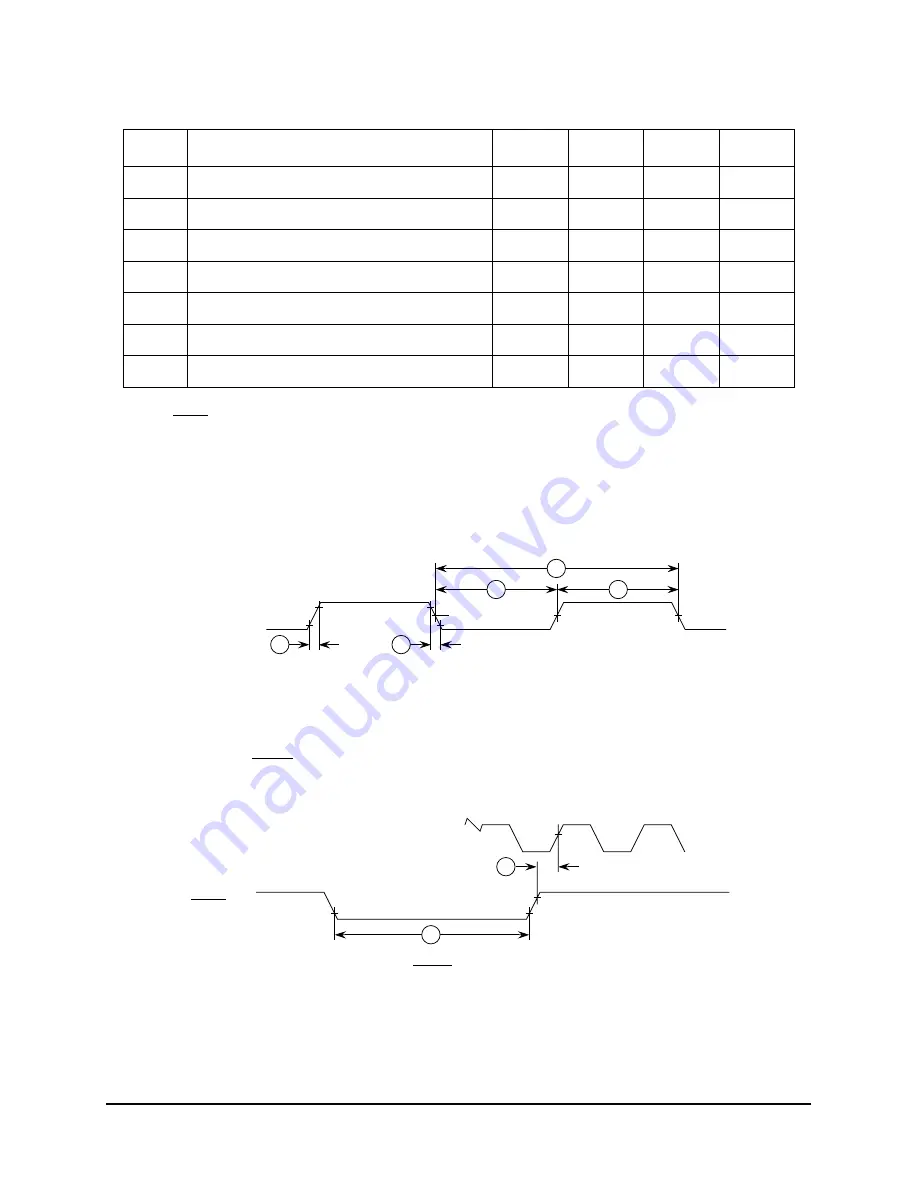
Figure 5 provides the JTAG clock input timing diagram.
Figure 5. Clock Input Timing Diagram
Figure 6 provides the TRST timing diagram
.
Figure 6. TRST Timing Diagram
7
Boundary-scan input data hold time
27
—
ns
2
8
TCK to output data valid
4
25
ns
3
9
TCK to output high impedance
3
24
ns
3
10
TMS, TDI data setup time
0
—
ns
11
TMS, TDI data hold time
25
—
ns
12
TCK to TDO data valid
4
24
ns
13
TCK to TDO high impedance
3
15
ns
Notes:
1. TRST is an asynchronous signal. The setup time is for test purposes only.
2. Non-test signal input timing with respect to TCK.
3. Non-test signal output timing with respect to TCK.
Table 9. JTAG AC Timing Specifications (Independent of SYSCLK) (Continued)
Vdd = 3.3
±
5% V dc, GND = 0 V dc, C
L
= 50 pF, 0
≤
T
j
≤
105
°
C
Num
Characteristic
Min
Max
Unit
Notes
TCK
2
2
1
VM
VM
VM
3
3
VM = Midpoint Voltage (1.4 V)
4
5
TRST
TCK
VM


