Chapter 7. PCI Bus Interface
7-23
PCI Bus Transactions
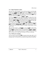
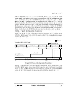
7.4.5.2 Accessing the PCI Configuration Space
This section describes accessing the external PCI configuration space. See Section 7.7.2,
“Accessing the MPC8240 Configuration Space,” for information on accessing the internal
configuration registers of the MPC8240.
To support hierarchical bridges, two types of configuration accesses are supported. The first
type of configuration access, type 0, is used to select a device on the local PCI bus. Type 0
configuration accesses are not propagated beyond the local PCI bus and must be claimed
by a local device or terminated with a master-abort. The second type of configuration
access, type 1, is used to pass a configuration request to another PCI bus (through a
PCI-to-PCI bridge). Type 1 accesses are ignored by all targets except PCI-to-PCI bridges.
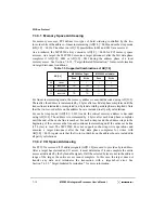
To access the configuration space, a 32-bit value must be written to the CONFIG_ADDR
register that specifies the target PCI bus, the target device on that bus, and the configuration
register to be accessed within that device. A read or write to the CONFIG_DATA register
causes the host bridge to translate the access into a PCI configuration cycle (provided the
enable bit in CONFIG_ADDR is set and the device number is not 0b1_1111).
For the MPC8240, the CONFIG_ADDR register is located at different addresses depending
on the memory address map in use. The address maps are described in Chapter 3, “Address
Maps.” For address map B, the processor can access the CONFIG_ADDR register at any
location in the address range from 0xFEC0_0000 to 0xFEDF_FFFF. For simplicity, the
address for CONFIG_ADDR is sometimes referred to as CF8, 0xnnnn_nCF8, or (in the
PCI literature as) CF8h. Although systems implementing address map B can use any
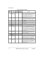
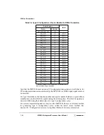
0x0E
Header type
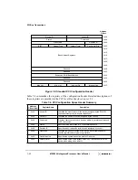
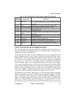
Bits 0–6 identify the layout of bytes 10–3F; bit 7 indicates a multifunction
device. The most common header type (0x00) is shown in Figure 7-8 and
in this table.
0x0F
BIST
Optional register for control and status of built-in self test (BIST)
0x10–0x27
Base address registers
Address mapping information for memory and I/O space
0x28
—
Reserved for future use
0x2C
—
Reserved for future use
0x30
Expansion ROM base
address
Base address and size information for expansion ROM contained in an
add-on board
0x34
—
Reserved for future use
0x38
—
Reserved for future use
0x3C
Interrupt line
Contains interrupt line routing information
0x3D
Interrupt pin
Indicates which interrupt pin the device (or function) uses
0x3E
Min_Gnt
Specifies the length of the device’s burst period in 0.25 µs units
0x3F
Max_Lat
Specifies how often the device needs to gain access to the bus in 0.25
µs units
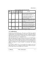
Table 7-4. PCI Configuration Space Header Summary (Continued)
Address
Offset (Hex)
Register Name
Description
Содержание MPC8240
Страница 1: ...MPC8240UM D Rev 1 1 2001 MPC8240 Integrated Processor User s Manual ...
Страница 38: ...xviii MPC8240 Integrated Processor User s Manual TABLES Table Number Title Page Number ...
Страница 48: ...xlviii MPC8240 Integrated Processor User s Manual Acronyms and Abbreviations ...
Страница 312: ...6 94 MPC8240 Integrated Processor User s Manual ROM Flash Interface Operation ...
Страница 348: ...7 36 MPC8240 Integrated Processor User s Manual PCI Host and Agent Modes ...
Страница 372: ...8 24 MPC8240 Integrated Processor User s Manual DMA Register Descriptions ...
Страница 394: ...9 22 MPC8240 Integrated Processor User s Manual I2O Interface ...
Страница 412: ...10 18 MPC8240 Integrated Processor User s Manual Programming Guidelines ...
Страница 454: ...12 14 MPC8240 Integrated Processor User s Manual Internal Arbitration ...
Страница 466: ...13 12 MPC8240 Integrated Processor User s Manual Exception Latencies ...
Страница 516: ...16 14 Watchpoint Trigger Applications ...
Страница 538: ...B 16 MPC8240 Integrated Processor User s Manual Setting the Endian Mode of Operation ...
Страница 546: ...C 8 MPC8240 Integrated Processor User s Manual ...
Страница 640: ...INDEX Index 16 MPC8240 Integrated Processor User s Manual ...

