background image

A-2

Computer Group Literature Center Web Site

Specifications

A

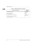
Cooling Requirements

The Motorola MCPN750A family of Single Board Computers is specified, 
designed, and tested to meet thermal performance requirements when 
installed in a properly designed CompactPCI chassis and supplied with 55 
degree C air flow at sea level. Tests were conducted with a Motorola 
CPX8216 system. Case temperatures of critical, high power density 
integrated circuits are monitored to ensure component vendors’ 
specifications are not exceeded.

The MCPN750A has been shown to operate reliably with an average air 
flow measurement of 355 LFM on the primary side of the board, and 450 
LFM on the secondary side of the board. Under these circumstances, all 
devices on the board operated within the vendor’s temperature 
requirements as noted in the manufacturer’s specification.

Содержание MCPN750A

Страница 1: ... underutilized and idle equipment along with credit for buybacks and trade ins Custom engineering so your equipment works exactly as you specify Critical and expedited services Leasing Rentals Demos In stock Ready to ship TAR certified secure asset solutions Expert team I Trust guarantee I 100 satisfaction All trademarks brand names and brands appearing herein are the property of their respective ...

Страница 2: ...MCPN750A CompactPCI Single Board Computer Installation and Use MCPN750A IH5 September 2001 Edition ...

Страница 3: ...orola Inc PowerPC is a registered trademark of International Business Machines and is used by Motorola Inc under license from IBM Corporation CompactPCI is a registered trademark of PCI Industrial Computer Manufacturers Group All other product or service names mentioned in this document are trademarks or registered trademarks of their respective holders ...

Страница 4: ...ide the Equipment Operating personnel must not remove equipment covers Only Factory Authorized Service Personnel or other qualified service personnel may remove equipment covers for internal subassembly or component replacement or any internal adjustment Service personnel should not replace components with power cable connected Under certain conditions dangerous voltages may exist even with the po...

Страница 5: ...losion if battery is replaced incorrectly Replace battery only with the same or equivalent type recommended by the equipment manufacturer Dispose of used batteries according to the manufacturer s instructions Attention Il y a danger d explosion s il y a remplacement incorrect de la batterie Remplacer uniquement avec une batterie du même type ou d un type équivalent recommandé par le constructeur M...

Страница 6: ...ilable on request Please contact your sales representative Notice While reasonable efforts have been made to assure the accuracy of this document Motorola Inc assumes no liability resulting from any omissions in this document or from the use of the information obtained therein Motorola reserves the right to revise this document and to make changes from time to time in the content hereof without ob...

Страница 7: ...d to in writing by Motorola Inc Use duplication or disclosure by the Government is subject to restrictions as set forth in subparagraph b 3 of the Rights in Technical Data clause at DFARS 252 227 7013 Nov 1995 and of the Rights in Noncommercial Computer Software and Documentation clause at DFARS 252 227 7014 Jun 1995 Motorola Inc Computer Group 2900 South Diablo Way Tempe Arizona 85282 ...

Страница 8: ...h Bank Selection J7 1 7 Stand Alone Operating Mode J8 1 8 System Considerations 1 10 TMCPN710 Transition Module Preparation 1 11 Serial Ports 1 and 2 1 13 COM3 and COM4 Asynchronous Serial Ports 1 15 TM PIMC 0001 Transition Module Preparation 1 16 COM 1 and COM 2 Asynchronous Serial Ports 1 18 COM3 and COM4 Asynchronous Serial Ports 1 20 Hardware Installation 1 21 Installing PMC Modules on the MCP...

Страница 9: ...ation 2 8 Interrupt Handling 2 8 ISA DMA Channels 2 9 Sources of Reset 2 9 Power On Reset 2 11 Undervoltage Reset 2 11 Front Panel Push Button Reset 2 11 CompactPCI Reset RST 2 11 Watchdog Timer Reset 2 11 Software Resets 2 12 Reset Source Identification 2 12 Endian Issues 2 12 Processor Memory Domain 2 12 PCI Domain 2 13 CHAPTER 3 PPCBug PPCBug Overview 3 1 PPCBug Basics 3 1 Memory Requirements 3...

Страница 10: ...x05 Memory Size Query 5 7 Opcode 0x06 Debugger Query 5 7 Opcode 0x07 Execute Code 5 7 Command Response Channel Error Codes 5 8 Demonstration of the Host Interface 5 9 Reference Function srom_crc c 5 12 CHAPTER 6 Functional Description Introduction 6 1 Features 6 1 General Description 6 2 Block Diagram 6 3 CompactPCI Bus Interface 6 5 Ethernet Interface 6 6 PCI Mezzanine Interface 6 7 ISA Bus Devic...

Страница 11: ... Bank A Flash Programming Enable 6 21 ECC Memory Controller 6 22 DRAM Memory 6 22 Compact FLASH Memory Card 6 22 TMCPN710 Transition Module 6 23 TM PIMC 0001 6 23 CHAPTER 7 Connector Pin Assignments MCPN750A and Transition Module Connectors 7 1 MCPN750A Connector Pin Assignments 7 2 MCPN750A CompactPCI Bus Connectors J1 J2 7 2 MCPN750A CompactPCI User I O Connector J3 7 4 MCPN750A Connector J4 7 6...

Страница 12: ...Module 7 27 TM PIMC 0001 CompactPCI User I O Connector J3 J4 J5 7 27 TM PIMC 0001 Transition Module COM1 Connector J9 7 28 TM PIMC 0001 Transition Module COM2 Connector J8 7 29 TM PIMC 0001 Transition Module COM3 and COM4 Connectors J12 J13 7 30 TM PIMC 0001 Transition Module 10BaseT 100BaseTx Connector J7 7 31 TM PIMC 0001 Transition Module IDE Compact FLASH Connector J1 7 31 TM PIMC 0001 Transit...

Страница 13: ...xii ...

Страница 14: ...ial Ports 3 and 4 1 15 Figure 1 6 TM PIMC 0001 Connector and Header Locations 1 17 Figure 1 7 MCPN750A TM PIMC 0001 Serial Ports 1 and 2 1 19 Figure 1 8 TM PIMC 0001 Serial Ports 3 and 4 1 20 Figure 1 9 PMC Module Placement on MCPN750A 1 22 Figure 1 10 TMCPN710 or TM PIMC 0001 MCPN750A Mating Configuration 1 30 Figure 2 1 PPCBug System Startup 2 2 Figure 6 1 MCPN750A Block Diagram 6 4 Figure 6 2 S...

Страница 15: ...xiv ...

Страница 16: ...100BaseTx Connector J18 7 12 Table 7 8 MCPN750A Debug Connector J19 7 13 Table 7 9 MCPN750A RISCWatch Debug Connector J6 7 17 Table 7 10 TMCPN710 COM1 Connector J6 7 19 Table 7 11 TMCPN710 COM2 Connector J8 7 20 Table 7 12 TMCPN710 COM3 COM4 Headers 7 20 Table 7 13 TMCPN710 10BaseT 100BaseTx Connector J13 7 22 Table 7 14 TMCPN710 USB 0 Connector J10 7 23 Table 7 15 TMCPN710 USB 1 Connector J12 7 2...

Страница 17: ...dules 1 and 2 PIM1 and PIM2 PMC I O Connector Pin Assignments 7 36 Table A 1 MCPN750 Specifications A 1 Table B 1 Motorola Computer Group Documents B 1 Table B 2 Manufacturers Documents B 2 Table B 3 Related Specifications B 4 ...

Страница 18: ...re provided in the following configurations Part Number Description MCPN750 1222A MPC750 266MHz 16MB ECC DRAM 5MB FLASH 1MB L2 Cache MCPN750 1232A MPC750 266MHz 32MB ECC DRAM 5MB FLASH 1MB L2 Cache MCPN750 1332A MPC750 366MHz 32MB ECC DRAM 5MB FLASH 1MB L2 Cache MCPN750 1342A B MPC750 366MHz 64MB ECC DRAM 5MB FLASH 1MB L2 Cache MCPN750 1352A B MPC750 366MHz 128MB ECC DRAM 5MB FLASH 1MB L2 Cache MC...

Страница 19: ...ring issues such as the PPCBug firmware the memory maps interrupts arbitration sources of reset and endian issues Chapter 3 PPCBug provides an overview and description of basic PPCBug use including implementation issues a list of the initialization sequence a description of basic debugger commands as well as a list of diagnostic tests typically run Date Changes Replaces 09 01 Updated table of mode...

Страница 20: ...ting of all major connector pinout information for the MCPN750A the TMCPN710 and TM PIMC 0001 Appendix A Specifications provides basic board specification information including recommendations on cooling and EMC compliance Appendix B Related Documentation provides a listing of related motorola and vendor documentation as well as a list of related industry standard specifications Comments and Sugge...

Страница 21: ...t you type just as it appears it is also used for commands options and arguments to commands and names of programs directories and files italic is used for names of variables to which you assign values Italic is also used for comments in screen displays and examples and to introduce new terms courier is used for system output for example screen displays reports examples and system prompts Enter Re...

Страница 22: ... PMC for additional versatility One of two different types of optional transition modules the TMCPN710 or the TM PIMC 0001 for added I O flexibility Product Description The MCPN750A is a hot swappable CompactPCI non system slot single board computer based on the PowerPlus architecture It consists of the MPC750 processor with L2 cache the Raven PCI Bridge and Interrupt Controller the ECC Memory Con...

Страница 23: ...ASIC DRAM Bank 1 16M 64M 128M SROM AT24C04 Interrupt Serializer DRAM Bank 2 16M 64M 128M Flash soldered 4M Flash socketed 1M System Registers Clock Generator Reset Control ISA Registers Hot Swap Control Ethernet Intel 21143 PBC VT82C586B PCI PCI BRIDGE Intel 21554 32 64 bit PMC Slot 1 33MHz 32 64 bit CompactPCI Bus CompactPCI J1 J2 User I O J3 J5 UARTs 16C550C MK48T559 10BT 100BTx RS232 IOMX Debug...

Страница 24: ...e you begin Table 1 1 Startup Overview Task Section or Manual Reference Page Unpack the hardware Unpacking Instructions 1 5 Configure the hardware by setting jumpers on the baseboard and transition module MCPN750A Baseboard Preparation and TMCPN710 or TM PIMC 0001 Transition Module Preparation 1 6 1 11 and 1 16 Ensure CompactFlash card is installed if required Compact Flash Memory Card Installatio...

Страница 25: ...s and front or rear ethernet I O Either one of the aforementioned transition modules support all models of the baseboard Refer to the subsections on the MCPN750A and transition module installation for more information Note that the debugger initializes the MCPN750A Using PPCBug 3 5 You may also wish to obtain the PPCBug Firmware Package User s Manual listed in Appendix B Related Documentation B 1 ...

Страница 26: ...when installing or upgrading a system Electronic components such as disk drives computer boards and memory modules can be extremely sensitive to ESD After removing the component from the system or its protective wrapper place the component flat on a grounded static free surface and in the case of a board component side up Do not slide the component over any surface If an ESD station is not availab...

Страница 27: ...ngle Board Computer Programmer s Reference Guide MCPN750A PG which can be accessed on line in pdf or html format through the Motorola Computer Group Literature web site http www motorola com computer literature Some options however are not software programmable These options are controlled by installing or removing header jumpers or interface modules on the baseboard or the associated transition m...

Страница 28: ...memory The Flash memory is organized in two banks Bank A is 64 bits wide and Bank B is 16 bits wide Bank B contains the onboard debugger PPCBug To enable Flash Bank A place a jumper across header J7 pins 1 and 2 To enable Flash Bank B 1MB of firmware located in sockets on the baseboard place a jumper across header J7 pins 2 and 3 Note Placing a jumper on Flash programming header J9 has no affect T...

Страница 29: ...talling a jumper across pins 1 and 2 of J8 enables the stand alone mode The J8 jumper must be removed for normal operation Note An MCPN750A configured for stand alone mode should not be installed in a chassis with a system slot controller board This will result in unpredictable system operation See the section on System Considerations for additional information 2 1 2 1 Enables Stand Alone mode Rem...

Страница 30: ... 100 BASE T 2 ABT RST BFL CPU PCI MEZZANINE CARD 2 1 15 16 J21 64 63 S1 J6 1 2 2 1 J22 64 63 J5 J4 J3 J2 J1 2 1 J23 64 63 2 1 J24 64 63 2 1 J11 64 63 2 1 J12 64 63 2 1 J13 64 63 2 1 J14 64 63 J7 3 1 XU1 XU2 J18 J19 U23 U20 U31 Q3 Q4 L2 U35 U2 U1 U5 U9 U8 U7 U6 U16 U15 U14 U13 U12 J9 3 1 COM 1 PCI MEZZANINE CARD 1 DS2 DS1 DS3 J8 2 1 ...

Страница 31: ...input This allows the MCPN750A to operate in a chassis without a system slot controller board installed The chassis must provide 5V 3 3V 12V 12V and VIO to the MCPN750A and the BD_SEL pin P1 D15 in the chassis must be grounded In addition in the stand alone mode the MCPN750A cannot communicate over the CompactPCI backplane On the MCPN750A baseboard the standard serial console port COM1 serves as t...

Страница 32: ...f the TMCPN710 include Two EIA 232 D asynchronous serial ports identified as COM1 and COM2 on the transition module panel Two USB Series A connectors for USB interface One 10 100BaseT connector for ethernet connections requires MCPN750A Transition module ethernet option Two 68 pin 08 Series Subminiature D connectors for PMC I O Two 50 pin on board connectors for EIDE interface to one or two Compac...

Страница 33: ...ware Preparation and Installation 1 Figure 1 3 TMCPN710 Connector and Header Locations 2286 9806 COM 2 USB 1 PMC1 I O 4 1 J13 J10 J12 4 1 8 2 7 1 10 100 BASE T J8 8 2 7 1 COM 1 PMC2 I O USB 0 J3 J5 J4 J6 8 2 7 1 J15 J16 J7 1 3 J2 J1 J11 J14 Master Slave ...

Страница 34: ...ected to either the processor board or the transition module but not both Jumper J7 on the transition module must be configured to enable COM1 on either the transition module or the processor board To enable the COM1 port on the transition module connect pins 2 3 of J7 To enable COM1 on the processor board connect pins 1 2 of J7 Note If the J7 jumper is not present on the TMCPN710 the board automa...

Страница 35: ...ion 1 Figure 1 4 MCPN750A TMCPN710 Serial Ports 1 and 2 2362 9808 SOUT SIN RTS CTS RI DTR DCD DSR 16C550 J7 J3 1 7 2 8 5 4 3 6 RI DSR DCD DTR SOUT CTS RTS SIN 16C550 1 8 2 5 7 4 3 6 IO MUX RJ45 front panel COM1 rear panel COM1 4 5 7 8 2 1 3 6 rear panel COM2 TMCPN710 MCPN750A IO MUX ...

Страница 36: ...s on the TMCPN710 Transition Module These headers are intended for debug purposes only Figure 1 5 depicts this configuration Figure 1 5 TMCPN710 Serial Ports 3 and 4 2363 9808 SOUT SIN RTS CTS RI DTR DCD DSR 16C550 J3 RI DSR DCD DTR SOUT CTS RTS SIN 16C550 3 5 9 14 7 15 11 18 TMCPN710 MCPN750A IO MUX Com4 Header Com3 Header J11 J14 IO MUX 13 18 11 14 9 15 7 5 3 13 ...

Страница 37: ...ll models of the MCPN750A baseboard The features of this transition module include Connections for two single wide or one double wide PIM card Two asynchronous serial ports using RJ 45 connectors labeled as COM1 and COM2 Two asynchronous serial ports using 10 pin headers labeled as COM3 and COM4 One ethernet port using an RJ 45 connector One IDE Flash connector using a standard 50 pin CompactFlash...

Страница 38: ...ure 1 6 TM PIMC 0001 Connector and Header Locations J8 8 2 7 1 2694 0001 COM 2 3 1 COM 1 8 1 J16 J3 J5 J4 J9 8 2 7 1 J7 8 2 7 1 3 1 J2 2 63 64 J20 1 2 63 64 J24 1 2 63 64 J10 1 2 63 64 J14 1 J1 J11 10 100 BASE T PMC I O MODULE 1 PMC I O MODULE 2 J13 J12 1 2 9 1 2 9 ...

Страница 39: ... COM1 may be connected to either the processor board or the transition module but not both Jumper J11 on the transition module must be configured to enable COM1 on the processor board If J11 is not configured COM1 is automatically routed to PIM 1 on the transition module Jumper J2 on the transition module must be configured in the same way for the COM2 port 2 3 J11 1 2 3 J11 Serial Port 1 jumper s...

Страница 40: ...C 0001 Serial Ports 1 and 2 2362 0001 SOUT SIN RTS CTS RI DTR DCD DSR 16C550 J11 J3 1 7 2 8 5 4 3 6 RI DSR DCD DTR SOUT CTS RTS SIN 16C550 1 8 2 5 7 4 3 6 IO MUX RJ45 front panel COM1 rear panel COM1 4 5 7 8 2 1 3 6 rear panel COM2 TM PIMC 0001 MCPN750 IO MUX IO MUX PIM 1 IO MUX PIM 2 J2 ...

Страница 41: ...IMC 0001 Transition Module J12 and J13 These headers function as I O connectors for the MCPN750A and are permanently configured as DTE Figure 1 8 depicts this configuration Figure 1 8 TM PIMC 0001 Serial Ports 3 and 4 2363 0001 SOUT SIN RTS CTS RI DTR DCD DSR 16C550 J3 RI DSR DCD DTR SOUT CTS RTS SIN 16C550 5 3 6 7 4 1 2 8 TM PIMC 0001 MCPN750A IO MUX Com4 Header Com3 Header J12 J13 IO MUX 9 8 2 7...

Страница 42: ...p 4 Caution Avoid touching areas of integrated circuitry static discharge can damage these circuits Installing PMC Modules on the MCPN750A SBC One dual wide one single wide or two single wide PCI mezzanine PMC modules can be mounted on top of the MCPN750A baseboard The MCPN750A is designed to accept only 5V or Universal PMCs Due to pin current limitations the MCPN750A can supply up to 4 5 amps to ...

Страница 43: ... with power applied may result in damage to module components The MCPN750A is a hot swappable board and may be inserted in a hot swap chassis such as a CPX2000 or a CPX8000 series chassis with power applied Warning Dangerous voltages capable of causing death are present in this equipment Use extreme caution when handling testing and adjusting 4 Carefully remove the MCPN750A from its CompactPCI car...

Страница 44: ...ors J11 12 13 14 on the MCPN750A 7 Insert the four short Phillips screws provided with the PMC through the holes on the bottom side of the MCPN750A into the PMC front bezel and rear standoffs Tighten the screws 8 Reinstall the MCPN750A assembly in its proper card slot Be sure the module is well seated in the backplane connectors Do not damage or bend connector pins 9 Replace the chassis or system ...

Страница 45: ...Caution Inserting or removing modules in a non hot swap chassis with power applied may result in damage to module components The MCPN750A is a hot swappable board and may be inserted in a hot swap chassis such as a CPX2000 or a CPX8000 series chassis with power applied Dangerous voltages capable of causing death are present in this equipment Use extreme caution when handling testing and adjusting ...

Страница 46: ...ese circuits 6 Secure the MCPN750A in the chassis with the screws provided making good contact with the transverse mounting rails to minimize RF emissions 7 Replace the chassis or system cover s making sure no cables are pinched Cable the peripherals to the panel connectors reconnect the system to the AC or DC power source and turn the equipment power on ...

Страница 47: ... Use TMPIMCA IH manual Installing PIMs on the TM PIMC 0001 Transition Module If PIMs have already been installed on the TM PIMC 0001 or you are installing a transition module as it has been shipped from the factory disregard this section and proceed to the main installation section titled Installing the Transition Module in the Chassis For PIM installation perform the following steps 1 Attach an E...

Страница 48: ...ule Caution Inserting or removing modules in a non hot swap chassis with the power applied may result in damage to the module components The TM PIMC 0001 is not a hot swap board but it may be installed in a hot swap chassis with power applied if the corresponding MCPN750A is removed before the TM PIMC 0001 board is installed 2695 0001 ...

Страница 49: ...IMC 0001 7 Insert the four short Phillips screws provided with the PIM through the holes on the bottom side of the TM PIMC 000 into the PIM front bezel and rear standoffs Tighten the screws 8 Reinstall the TM PIMC 0001 assembly in its proper card slot Be sure the module is well seated in the backplane connectors Do not damage or bend connector pins 9 Replace the chassis or system cover s reconnect...

Страница 50: ...n positioning of the corresponding MCPN750A board carefully slide the transition module into the appropriate slot and seat tightly into the backplane Refer to Figure 1 11 TMCPN710 or TM PIMC 0001 MCPN750A Mating Configuration for the correct board connector orientation 4 Secure in place with the screws provided making good contact with the transverse mounting rails to minimize RF emissions 5 Repla...

Страница 51: ...Computer Group Literature Center Web Site Hardware Preparation and Installation 1 Figure 1 11 TMCPN710 or TM PIMC 0001 MCPN750A Mating Configuration MCPN750A TMCPN710 or TM PIMC 0001 P1 P2 P3 P4 P5 P3 P4 P5 ...

Страница 52: ...PN750A hot swap controller and provided for use by the PMCs and transition modules The MCPN750A contains an electronic circuit breaker that limits the total 5V 3 3V 12V and 12V current drawn by the MCPN750A Refer to the table below for the electrical current available to the PMCs and transition modules and Appendix A for other specs Voltage Current Available to PMCs Transition Modules 5 0V 6 Amps ...

Страница 53: ...1 32 Computer Group Literature Center Web Site Hardware Preparation and Installation 1 ...

Страница 54: ...e you can power up the system The MPU hardware and firmware initialization process is performed by the PowerPC PPCBug power up or system reset The firmware initializes the devices on the SBC module in preparation for booting the operating system The firmware is shipped from the factory with an appropriate set of defaults In most cases there is no need to modify the firmware configuration before yo...

Страница 55: ...anel has one ABORT RESET switch and three LED light emitting diode status indicators BFL CPU and HOT SWAP STATUS For more information on front panel operation refer to Chapter 6 Functional Description STARTUP SYSTEM INITIALIZATION CONSOLE DETECTION OPERATING SYSTEM RUN SELFTESTS IF ENABLED AUTOBOOT IF ENABLED 11734 00 9702 ...

Страница 56: ...he processor memory map configuration is under the control of the Raven bridge controller ASIC and the Falcon memory controller chip set The Raven and Falcon devices adjust system mapping to suit a given application via programmable map decoder registers At system power up or reset a default processor memory map takes over Default Processor Memory Map The default processor memory map that is valid...

Страница 57: ...ber MCPN750A PG PCI Local Bus Memory Map The local PCI memory map is the PCI memory map as viewed by the MCPN750A base board This is also the secondary bus side of the 21554 on the MCPN750A This map is controlled by the Raven ASIC and the 21554 PCI to PCI bridge The Raven and the 21554 PCI to PCI bridge have flexible programmable map decoder registers to customize the system for a wide range of ap...

Страница 58: ...ements multiple base address registers on both the primary and secondary interfaces that denote separate address ranges for both downstream and upstream transactions It also has base registers for access to its Control and Status Register CSR space Consequently on the primary interface CompactPCI bus the 21554 responds only to those transactions which are in the address range defined by one of the...

Страница 59: ...PG for additional information System Clock Generator The system clocks for the processor Raven Falcon chipset 66 MHz and each of the onboard PCI devices 33 MHz are generated by a 66 MHz oscillator and distributed by the MPC949 clock buffer Separate oscillators are provided as follows 14 31818 MHz for the PBC internal timer 20 MHz for the ethernet MAC interface 25 MHz for the ethernet PHY device 48...

Страница 60: ...onnected to the processor data parity signals to provide processor data bus parity generation and checking There are four programmable map decoders for each direction to provide flexible address mappings between the PPC DRAM and the PCI Local Bus Refer to the MCPN750A CompactPCI Single Board Computer Programmer s Reference Guide MCPN750A PG for additional information and programming details ...

Страница 61: ...x other interrupt sources inside the MPIC Two cross processor interrupts and four timer interrupts All ISA interrupts go through the 8259 pair in the Peripheral Bus Controller PBC The output of the PBC then goes through the MPIC in Raven Since the MCPN750A board is designed to support processor data bus parity the Raven uses some of the pins normally used as external interrupt inputs as parity pin...

Страница 62: ...ammer s Reference Guide MCPN750A PG ISA DMA Channels The PBC supports seven 8237 compatible DMA channels ISA compatible type A B and F timing is supported These DMA channels are not used since there are no ISA DMA devices Sources of Reset The MCPN750A SBC provides reset control from various sources and identifies the source of the reset in a software readable register Hard or soft resets may be ge...

Страница 63: ...pactPCI Single Board Computer Programmer s Reference Guide part number MCPN750A PG 21554 Secondary Reset Bit does not reset the 21554 register state but does reset the 21554 data buffers A configuration write is required to clear the Secondary Reset Bit after it has been written so this bit must not be set by the local MCPN750A processor or else the board will lock up Table 2 2 Classes of Reset an...

Страница 64: ... reset is maintained for 140 to 560 milliseconds after the voltages have returned to the minimum threshold For undervoltage the Vcc threshold to reset delay is typically 10 microseconds Front Panel Push Button Reset The front panel RESET switch generates a hard reset when depressed for more than three 3 seconds The reset is maintained as long as the switch is depressed CompactPCI Reset RST The Com...

Страница 65: ...set by reading the Reset Source register Refer to the MCPN750A CompactPCI Single Board Computer Programmer s Reference Guide MCPN750A PG for bit assignments Endian Issues The MCPN750A supports both little endian and big endian software The PowerPC is inherently big endian while the PCI bus is inherently little endian The following sections summarize how the MCPN750A handles software and hardware d...

Страница 66: ...esses from PCI In this case no byte swapping is done PCI Domain The PCI bus is inherently little endian All devices connected directly to the PCI bus operate in little endian mode regardless of the mode of operation in the processor s domain PCI and Ethernet Ethernet is also byte stream oriented the byte having the lowest address in memory is the first one to be transferred regardless of the endia...

Страница 67: ...2 14 Computer Group Literature Center Web Site Startup and Operation 2 ...

Страница 68: ...lls and other advanced user topics For full user information about PPCbug refer to the PPCBug Firmware Package User s Manual and the PPCBug Diagnostics Manual listed in the Related Documentation appendix PPCBug Basics The PowerPC debug firmware PPCBug is a powerful evaluation and debugging tool for systems built around the Motorola PowerPC microcomputers Facilities are available for loading and ex...

Страница 69: ...ystem console terminal When using PPCBug you operate out of either the debugger directory or the diagnostic directory If you are in the debugger directory the debugger prompt PPC1 Bug is displayed and you have all of the debugger commands at your disposal If you are in the diagnostic directory the diagnostic prompt PPC1 Diag is displayed and you have all of the diagnostic commands at your disposal...

Страница 70: ...d Physically PPCBug is contained in two socketed 32 pin PLCC Flash devices that together provide 1MB of storage The executable code is checksummed at every power on or reset firmware entry and the result which includes a precalculated checksum contained in the Flash devices is verified against the expected checksum MPU Hardware and Firmware Initialization The debugger performs the MPU hardware and...

Страница 71: ...ash from NVRAM 16 Initializes the read only memory controller with the speed of read only memory 17 Enables the MPU s instruction cache 18 Copies the MPU s exception vector table from FFF00000 to 00000000 19 Verifies MPU type 20 Enable the super scalar feature of the MPU boards with MPC750 type chips only 21 Determines the debugger s console host ports and initializes the appropriate devices PC165...

Страница 72: ...torage devices 31 Initializes the memory IO addresses for the supported PCI bus devices 32 Executes Self Test if so configured Default is no Self Test 33 Extinguishes the board fail LED if there are no self test failures or initialization configuration errors 34 Executes the configured boot routine either ROMboot Autoboot or Network Autoboot 35 Executes the user interface i e displays the PPC1 Bug...

Страница 73: ...dler routine RETURN described in the PPCBug Firmware Package User s Manual Chapter 5 For more about this refer to the GD GO and GT command descriptions in the PPCBug Firmware Package User s Manual Chapter 3 A debugger command is made up of the following parts The command name either uppercase or lowercase e g MD or md Any required arguments as specified by command At least one space before the fir...

Страница 74: ...d by a carriage return Table 3 1 Debugger Commands Command Description AS One Line Assembler BC Block of Memory Compare BF Block of Memory Fill BI Block of Memory Initialize BM Block of Memory Move BR Breakpoint Insert NOBR Breakpoint Delete BS Block of Memory Search BV Block of Memory Verify CACHE Disable Enable Cache CM Concurrent Mode NOCM No Concurrent Mode CNFG Configure Board Information Blo...

Страница 75: ...s Display GN Go to Next Instruction GO Go Execute User Program GT Go to Temporary Breakpoint HE Help IDLE Idle Master MPU IOC I O Control for Disk IOI I O Inquiry IOP I O Physical Direct Disk Access IOT I O Teach for Configuring Disk Controller IRD Idle MPU Register Display IRM Idle MPU Register Modify IRS Idle MPU Register Set LO Load S Records from Host MA Macro Define Display NOMA Macro Delete ...

Страница 76: ...trol NIOP Network I O Physical NIOT Network I O Teach Configuration NPING Network Ping OF Offset Registers Display Modify PA Printer Attach NOPA Printer Detach PBOOT Bootstrap Operating System PF Port Format NOPF Port Detach PFLASH Program FLASH Memory PS Put RTC into Power Save Mode RB ROMboot Enable NORB ROMboot Disable RD Register Display REMOTE Remote RESET Cold Warm Reset RL Read Loop RM Regi...

Страница 77: ...o use the diagnostics you must switch to the diagnostic directory You may switch between directories by using the SD Switch Directories command You may view a list of the commands in the directory that you are currently in by using the HE Help command RUN MPU Execution Status SD Switch Directories SET Set Time and Date SROM SROM Examine Modify SYM Symbol Table Attach NOSYM Symbol Table Detach SYMS...

Страница 78: ...es available in each test group Refer to the PPCBug Diagnostics Manual for complete descriptions of the diagnostic routines and instructions on how to invoke them Table 3 2 Diagnostic Test Groups Test Set Description CL1283 Parallel Interface CL1283 DEC DECchip 21x4x EIDE Tests ISABRDGE PCI ISA Bridge Tests KBD8730x PC8730x Keyboard Mouse Tests L2CACHE Level 2 Cache Tests NCR NCR 53C8xx SCSI 2 I O...

Страница 79: ... uppercase or lowercase Some diagnostics depend on restart defaults that are set up only in a particular restart mode Refer to the documentation on a particular diagnostic for the correct mode Test Sets marked with an asterisk are not available on the MCPN750A unless SCSI or Video PMCs are installed ...

Страница 80: ... the hardware Use the PPCBug command CNFG to change those parameters Use the PPCBug command ENV to change configured PPCBug parameters in NVRAM The CNFG and ENV commands are both described in the PPCBug Firmware Package User s Manual part number PPCBUGA1 UM Refer to that manual for general information about their use and capabilities The following paragraphs present additional information aboutCNF...

Страница 81: ...rings are right justified The data strings are padded with zeroes if the length is not met Note the MCPN750A has no local SCSI bus controller hence the Local SCSI Identifier parameter is ignored by the PPCBug The Board Information Block is factory configured before shipment There is no need to modify block parameters unless the NVRAM is corrupted Refer to the MCPN750A CompactPCI Single Board Compu...

Страница 82: ... can be configured using ENV are Bug or System environment B S B Field Service Menu Enable Y N N Probe System for Supported I O Controllers Y N Y B Bug is the mode where no system type of support is displayed However system related items are still available Default S System is the standard mode of operation and is the default mode if NVRAM should fail System mode is defined in the PPCBug Firmware ...

Страница 83: ...re set to the SCSI ID value entered here Y NVRAM PReP partition header space will be initialized automatically during board initialization but only if the PReP partition fails a sanity check Default N NVRAM header space will not be initialized automatically during board initialization Y Enable PReP style network booting same boot image from a network interface as from a mass storage device N Do no...

Страница 84: ... you the option of stopping the boot by use of the BREAK key The time value is from 0 255 seconds Default 5 seconds Auto Boot Enable Y N N Auto Boot at power up only Y N N Y Give boot priority to devices defined in the fw boot path global environment variable GEV N Do not give boot priority to devices listed in the fw boot path GEV Default Y Give boot priority to devices defined in the fw boot pat...

Страница 85: ...ition is to be booted as specified in the PowerPC Reference Platform PRP specification If set to zero the firmware will search the partitions in order 1 2 3 4 until it finds the first bootable partition That is then the partition that will be booted Other acceptable values are 1 2 3 or 4 In these four cases the partition specified will be booted without searching Auto Boot Abort Delay 7 The time i...

Страница 86: ... 255 seconds Default 5 seconds ROM Boot Direct Starting Address FFF00000 The first location tested when PPCBug searches for a ROMboot module Default FFF00000 ROM Boot Direct Ending Address FFFFFFFC The last location tested when PPCBug searches for a ROMboot module Default FFFFFFFC Network Auto Boot Enable Y N N Network Auto Boot at power up only Y N N Y The ROMboot function is enabled N The ROMboo...

Страница 87: ...rameters Offset NVRAM 00001000 The address where the network interface configuration parameters are to be saved retained in NVRAM these parameters are the necessary parameters to perform an unattended network boot A typical offset might be 1000 but this value is application specific Default 00001000 Caution If you use the NIOT debugger command these parameters need to be saved somewhere in the off...

Страница 88: ...nto the MPC105 ROMFAL field Memory Control Configuration Register 8 bits 23 27 to indicate the number of clock cycles used in accessing the ROM The lowest allowable ROMFAL setting is 00 the highest allowable is 1F The value to enter depends on processor speed refer to your specific processor and memory mezzanine module user s manual for appropriate values The default values vary according to the s...

Страница 89: ...errupts Route Control Registers PIRQ0 1 2 3 0A050900 Initializes the PIRQx PCI Interrupts route control registers in the IBC PCI ISA bus bridge controller The ENV parameter is a 32 bit value that is divided by 4 to yield the values for route control registers PIRQ0 1 2 3 The default is determined by system type For details on PCI ISA interrupt assignments and for suggested values to enter for this...

Страница 90: ...r A list of LED serial codes is included in the section on MPU Hardware and Firmware Initialization in Chapter 1 of the PPCBug Firmware Package User s Manual Part 1 A means to execute user selectable Bug commands upon Bug startup has been added to the ENV parameters The usage is as follows Firmware Command Buffer Enable Y N N Y Enables the Firmware Command Buffer execution N Disables the Firmware ...

Страница 91: ...ace into the command buffer should be typed just as you enter the commands from the command line The string NULL on a new line terminates the command line entries All BUG commands except for the following may be used within the command buffer DU ECHO LO TA VE Note Interactive editing of the startup command buffer is not supported If changes are needed to an existing set of startup commands a new s...

Страница 92: ...mand response channel This scratch pad register is logically divided into 5 sections An ownership flag When set indicates that the host owns the register and is free to write a new command into it It also indicates that the previous command if any has been completed and the results if any have been returned to the register When the host writes a new command to the register it must clear the owners...

Страница 93: ...he contents of the registers can be accessed via commands issued through the scratch register These registers are designated by the monikers VR0 VR1 VR2 and VR3 During reset startup the command response register is written with a specific reset pattern This indicates that the local CPU has been reset and is ready to accept commands through the command response register PPCBug uses certain areas of...

Страница 94: ...ccurred and the interface is ready to accept commands Bit 0 The ownership flag OWN A value of 1 indicates the host owns the register A value of 0 indicates that the local cpu owns the register Bits 1 to 7 7 bit command opcode field Each command is described in more detail in the following sections Bit 8 Global error status flag ERR If the command completed successfully then this bit will be writte...

Страница 95: ...compatibility with future implementations of this interface Note For most commands bit 9 is used to specify verbose non verbose mode target command processing In verbose mode command related information is printed on the target console as the host command is processed Verbose mode is selected when bit 9 0 non verbose mode is set when bit 9 1 Bits 16 to 31 16 bit data result field The meaning of th...

Страница 96: ...b00 VR0 0b01 VR1 0b10 VR2 0b11 VR3 This command cannot fail and will never set the ERR flag in the command response register Opcode 0x02 Initialize Memory This command allows the host to initialize areas of local RAM to a specific value without incurring the overhead of writing each location via the write memory command The command options field is unused and must contain 0 The lower 8 bits of the...

Страница 97: ...r the access is taken from VR0 Command option bits affect the operation as follows Bit 15 indicates read 0 or write 1 operation Bit 14 indicates whether to auto increment VR0 after the access is performed If 0 the contents of VR0 is unaffected by this command If 1 the contents of VR0 is incremented by 1 2 or 4 depending on the size of the access The autoincrement feature may be used during downloa...

Страница 98: ... of RAM that the firmware is using Information about the available RAM will return information which accounts for areas of RAM which the firmware is using Bit 14 specifies whether to return the beginning 0 or ending address 1 of the RAM Opcode 0x06 Debugger Query This command allows the host to determine the revision of the firmware present on the board The options field is unused and must contain...

Страница 99: ...es These are the 16 bit values that the target board returns in the Data Result field of the Command Response register when the target board detects an error in the processing of a host command These error codes are valid only if the ERR bit was set in the Command Response register Table 5 1 Command Respond Error Codes Error Code Associated Opcode Command Definition of the Error Code 0x0001 0x03 W...

Страница 100: ...example user interaction takes place on both the host and target consoles The console display examples are identified as MCP750 host Console and MCPN750A target Console respectively Note that reads and writes to the PCI Remote Start Command Response channel look a little unusual because the display is of the little endian representation of the data i e Command Channel data entered on the PPC1Bug c...

Страница 101: ...r PPC1 Bug Note In the program shown above you must manually adjust the operands of the instructions at memory locations 40218 and 4021C to produce a pointer to the Command Response register the 2155x Scratch 7 register that is appropriate for the particular target board you are using On the host console the PCI Remote Start Write Read virtual register command can be used to initialize VR0 and VR2...

Страница 102: ...007 cr PPC1 Bug The result of remote program execution can be viewed on the target console MCPN750A target Console PPC1 Bug Host wrote 0004 to upper half of VR0 Host wrote 0200 to lower half of VR0 Host wrote 0004 to upper half of VR2 Host wrote 0100 to lower half of VR2 GO 00040200 Effective address 00040200 YOU_DA_MAN PPC1 Bug ...

Страница 103: ... elements return CRC data unsigned int srom_crc elements_p elements_n register unsigned char elements_p buffer pointer register unsigned int elements_n number of elements register unsigned int crc register unsigned int crc_flipped register unsigned char cbyte register unsigned int index dbit msb crc 0xffffffff for index 0 index elements_n index cbyte elements_p for dbit 0 dbit 8 dbit msb crc 31 1 ...

Страница 104: ...Introduction http www motorola com computer literature 5 13 5 crc_flipped 1 dbit crc 1 crc 1 crc_flipped dbit crc crc_flipped 0xffffffff return crc 0xffff ...

Страница 105: ...5 14 Computer Group Literature Center Web Site Remote Start Via the PCI Bus 5 ...

Страница 106: ...s Reference Guide MCPN750A PG Refer to it also for additional functional description information Features The following table summarizes the features of the MCPN750A single board computers Table 6 1 MCPN750A Features Feature Description Microprocessor MPC750 PowerPC processor ECC DRAM 16MB 256MB of memory through onboard DRAM devices L2 cache memory Populated with 1MB on base board Flash Memory Tw...

Страница 107: ...ynchronous serial ports a 512 x 8 Serial EEPROM an ISA slave interface a Fast EIDE interface and two PMC slots Functions provided from the ISA bus include a real time clock NVRAM serial ports and status registers Interrupts Software interrupt handling via Raven PCI MPU bridge and Peripheral Bus Controller Serial I O 1 async port COM1 via front panel 4 async ports via the transition module Ethernet...

Страница 108: ...nector for 10BaseT 100BaseTX Ethernet and an RJ45 connector for the asynchronous serial debug port COM1 Three additional serial ports two USB ports and the one EIDE channel are routed to J3 and J5 for transition module I O Another key feature of the MCPN750A family is the PCI Peripheral Component Interconnect bus In addition to the on board local bus peripherals the PCI bus supports an industry st...

Страница 109: ...k 1 16M 64M 128M SROM AT24C04 Interrupt Serializer DRAM Bank 2 16M 64M 128M FLASH soldered 4M FLASH socketed 1M System Registers Clock Generator Reset Control ISA Registers Hot Swap Control Ethernet Intel 21143 PBC VT82C586B PCI PCI BRIDGE Intel 21554 32 64 bit PMC Slot 1 33MHz 32 64 bit CompactPCI Bus CompactPCI J1 J2 User I O J3 J5 UARTs 16C550C MK48T559 10BT 100BTx RS232 IOMX Debug Connector IS...

Страница 110: ...eader and the configuration space is accessible from both primary and secondary buses Refer to the MCPN750A CompactPCI Single Board Computer Programmers Reference Guide MCPN750A PG for additional information and programming details The 21554 also provides for independent primary and secondary PCI clocks which means that the MCPN750A SBC has it s own local processor PCI bus clock source independent...

Страница 111: ...ion the Ethernet address is stored in the configuration area of the NVRAM specified by the Boot ROM and in the serial ROM attached to the 21143 These bytes are stored in bytes 0x14 through 0x19 in the Ethernet SROM The Ethernet information in the SROM is stored in DEC Version 3 format For further information on this refer to the Digital Semiconductor 21x4x Serial ROM Format Version 3 03 document U...

Страница 112: ...ernet ports The base board supports PMC front panel and rear transition module I O Two sets of four 64 pin connectors on the base board J11 J14 and J21 J24 interface with 32 bit or 64 bit IEEE P1386 1 PMC compatible mezzanines to add any desirable function The PCI Mezzanine Card slots have the following characteristics Refer to the Table on page 7 9 for the pin assignments of the PMC connectors Fo...

Страница 113: ...sition Module The other three serial port TTL signals are routed to the J3 I O connector only To save pins on the J3 connector the all Serial Port control lines routed through J3 are serialized using the IOMUX PLD Configuration and Status Registers The MCPN750A base board contains several registers used to provide configuration and status information about the board These registers are implemented...

Страница 114: ...re are no ISA DMA devices Interrupt controller functionality to support 14 ISA interrupts Edge level control for ISA interrupts Steerable PCI interrupts Note feature not used Interrupt steering via Raven ASIC Three interval counters timers 82C54 functionality Accesses to the configuration space for the PBC are performed by way of the CONADD and CONDAT Configuration Address and Data registers in th...

Страница 115: ... additional peripherals The PBC host controller completely supports the standard Universal Host Controller Interface UHCI Each USB port is routed to the J3 User I O connector to interface with the transition module The MCPN750A SBC provides monitoring for each USB channel VCC output Fusing for the USB VCC outputs is provided on the Transition Module Refer to the TM PIMC 0001 or the TMCPN710 Transi...

Страница 116: ...of non volatile static RAM a real time clock and a watchdog timer function This chip supplies a clock oscillator crystal power failure detection memory write protection 8KB of NVRAM and a battery in a package consisting of two parts A 28 pin 330mil SO device containing the real time clock RTC the oscillator power failure detection circuitry timer logic 8KB of static RAM SRAM and gold plated socket...

Страница 117: ...thium batteries Use the battery for its intended application only Note Do not recharge open puncture or crush incinerate expose to high temperatures or dispose of in your general trash collection To replace the lithium battery observe the following guidelines and follow the steps below Note When replacing the battery power must be applied to the board to prevent data loss Warning Dangerous voltage...

Страница 118: ...d touching areas of integrated circuitry static discharge can damage circuits Use ESD Wrist Strap Attach an ESD strap to your wrist Attach the other end of the ESD strap to an electrical ground Note that the system chassis may not be gro8unded if it is unplugged The ESD strap must be secured to your wrist and to ground throughout the procedure 1 To remove the battery from the module carefully pull...

Страница 119: ...ertion or impending removal of the board The state of this switch is monitored by the 21554 bridge chip which will assert the CompactPCI ENUM signal The ENUM signal indicates to the System Controller board either that the board has been inserted and is ready for configuration or that the board is about to be removed A blue LED is provided on the front panel to indicate when it is safe to remove th...

Страница 120: ...ds 2 seconds minimum using logic external to Raven Each timer must be disabled or reloaded by software to prevent a timeout Software may reload a new timer value or force the timer to reload a previously loaded value To disable or load reload a timer requires a two step process The first step is to write the pattern 55 to the timer register key field which will arm the timer register to enable an ...

Страница 121: ...es a refresh request signal for ISA memory This timer is not used in the MCPN750A Counter 2 provides the tone for the speaker output function on the PBC this timer output is not used in the MCPN750A The interval timers use the OSC clock input as their clock source The MCPN750A drives the OSC pin with a 14 31818 MHz clock source Serial Port Signal Multiplexing Due to pin limitations of the J3 conne...

Страница 122: ...I MXSYNC is asserted for one bit time at Time Slot 15 by the MCPN750A board MXSYNC is used by the transition module to synchronize with the MCPN750A board MXDO is the time multiplexed output line from the main board and MXDI is the time multiplexed line from the transition module A 16 to 1 multiplexing scheme is used with 10 MHz bit rate Sixteen Time Slots are defined and allocated as follows Seri...

Страница 123: ...h MXCLK s rising edge The timing relationships among MXCLK MXSYNC MXDO and MXDI are illustrated by the following figure Table 6 2 Multiplexing Sequence of the MX Function MXDO From MCPN750A MXDI From TMCPN710 TM PIMC 0001 TIME SLOT SIGNAL NAME TIME SLOT SIGNAL NAME 0 RTS3 0 CTS3 1 DTR3 1 DSR3 2 RTS1 2 DCD3 3 RTS2 3 CTS1 4 RTS4 4 RI3 5 DTR4 5 CTS4 6 Reserved 6 DSR4 7 Reserved 7 DCD4 8 Reserved 8 CT...

Страница 124: ...BORT ABT RESET RST Switch S1 The MCPN750A SBC contains a single push button switch that provides both ABORT and RESET functions When the switch is depressed for less than 3 seconds an interrupt is generated to the processor via ISA interrupts IRQ8 If the switch is held for more than 3 seconds a board hard reset is generated RTS3 DTR3 RTS1 RTS2 Reserved CTS3 DSR3 DCD3 CTS1 DCD2 MMXCLK MMXSYNC MMXDO...

Страница 125: ...ernal synchronous SRAMs for data storage The minimum processor speed is 266 MHz The maximum external processor bus speed is 66 MHz Processor data bus parity generation and check is supported in conjunction with the Raven Falcon chipset Raven PCI Host Bridge The Raven bridge controller ASIC provides the bridge between the MPC750 microprocessor bus and the PCI local bus Electrically the Raven chip i...

Страница 126: ...diagnostics Updating firmware ROM Under normal operation the Flash devices are in read only mode their contents are pre defined and they are protected against inadvertent writes due to loss of power conditions However for programming purposes programming voltage is always supplied to the devices and the Flash contents may be modified by executing the proper program command sequence Refer to Intel ...

Страница 127: ...em configuration registers Refer to the MCPN750A CompactPCI Single Board Computer Programmer s Reference Guide MCPN750A PG for additional information and programming details DRAM Memory The ECC DRAM memory consists of one or two banks which can be populated to provide 16MB 32MB 64MB 128MB or 256MB Each bank is populated with nine 16 bit wide 50 pin TSOP DRAM devices to form a 144 bit wide memory b...

Страница 128: ...for PMC I O For additional information about the serial interface modules refer to the TMCPN710 Transition Module Installation and Use manual listed in the Related Documentation appendix TM PIMC 0001 The TM PIMC 0001 transition module is used in conjunction with all models of the MCPN750A base board The transition module provides additional I O for the MCPN750A series of SBCs This transition modul...

Страница 129: ...e Center Web Site Functional Description 6 One standard 50 pin CompactFlash socket for IDE Flash For additional information about this transition module refer to the TM PIMC 0001 Transition Module Install and Use TMPIMCA IH manual ...

Страница 130: ...or J6 MCPN750A Compact FLASH Memory Card Connector TMCPN710 Transition Module COM1 Connector J6 TMCPN710 Transition Module COM2 Connector J8 TMCPN710 Transition Module COM3 Connector J11 and J14 TMCPN710 Transition Module 10BaseT 100BaseTx Connector J13 TMCPN710 Transition Module USB Connectors J10 J12 TMCPN710 Transition Module CompactFLASH IDE Connectors J15 J16 TMCPN710 Transition Module PMC I ...

Страница 131: ...3 3V or 5V J2 is 110 pin AMP Z pack 2mm hard metric type B connector Each of these connectors conform to the CompactPCI specification The pinout for connectors J1 and J2 are shown below Table 7 1 MCPN750A J1 CompactPCI Connector ROW A ROW B ROW C ROW D ROW E 25 5V REQ64_L ENUM_L 3 3V 5V 25 24 AD1 5V VIO AD0 ACK64_L 24 23 3 3V AD4 AD3 5V AD2 23 22 AD7 GND 3 3V AD6 AD5 22 21 3 3V AD9 AD8 GND CBE0_L ...

Страница 132: ...TCK 5V TMS TDO TDI 2 1 5V 12V TRST_L 12V 5V 1 Long Pin Short Pin Medium Pin Table 7 2 MCPN750A J2 CompactPCI Connector ROW A ROW B ROW C ROW D ROW E 22 GA4 GA3 GA2 GA1 GA0 22 21 No Connect CLK6 GND No Connect RSV No Connect RSV No Connect RSV 21 20 No Connect CLK5 GND No Connect RSV GND No Connect RSV 20 19 GND GND No Connect RSV No Connect RSV No Connect RSV 19 18 No Connect BRSVP2A18 No Connect ...

Страница 133: ... 16 15 No Connect BRSVP2A15 GND No Connect FAL_L No Connect REQ5_L No Connect GNT5_L 15 14 AD35 AD34 AD33 GND AD32 14 13 AD38 GND VIO AD37 AD36 13 12 AD42 AD41 AD40 GND AD39 12 11 AD45 GND VIO AD44 AD43 11 10 AD49 AD48 AD47 GND AD46 10 9 AD52 GND VIO AD51 AD50 9 8 AD56 AD55 AD54 GND AD53 8 7 AD59 GND VIO AD58 AD57 7 6 AD63 AD62 AD61 GND AD60 6 5 CBE5_L 64EN L VIO CBE4_L PAR64 5 4 VIO No Connect BR...

Страница 134: ...A UDATA0P 16 15 COM1RD COM2RD COM2TD USBV0_OK UDATA0N 15 14 3 3V 3 3V 3 3V 5V 5V 14 13 PMC1IO5 PMC1IO4 PMC1IO3 PMC1IO2 PMC1IO1 13 12 PMC1IO10 PMC1IO9 PMC1IO8 PMC1IO7 PMC1IO6 12 11 PMC1IO15 PMC1IO14 PMC1IO13 PMC1IO12 PMC1IO11 11 10 PMC1IO20 PMC1IO19 PMC1IO18 PMC1IO17 PMC1IO16 10 9 PMC1IO25 PMC1IO24 PMC1IO23 PMC1IO22 PMC1IO21 9 8 PMC1IO30 PMC1IO29 PMC1IO28 PMC1IO27 PMC1IO26 8 7 PMC1IO35 PMC1IO34 PMC...

Страница 135: ...a out signal to transition module I2CSCL I2 C Serial Clock for Transition Module SROM I2CSDA I2 C Serial Data for Transition Module SROM USBV0_OK USB Port 0 Voltage Monitor USBV1_OK USB Port 1 Voltage Monitor MCPN750A Connector J4 Connector J4 is installed on both the processor board and the transition module for mechanical alignment purposes only The keying tabs in the Type A connector assist wit...

Страница 136: ...DYA DA1 No Connect No Connect 19 18 DIOWA_L DA0 GND No Connect No Connect 18 17 GND DD14 DD15 DIORA_L DMARQA 17 16 DD9 DD10 DD11 DD12 DD13 16 15 DD5 DD6 GND DD7 DD8 15 14 DD0 DD1 DD2 DD3 DD4 14 13 PMC2IO5 PMC2IO4 PMC2IO3 PMC2IO2 PMC2IO1 13 12 PMC2IO10 PMC2IO9 PMC2IO8 PMC2IO7 PMC2IO6 12 11 PMC2IO15 PMC2IO14 PMC2IO13 PMC2IO12 PMC2IO11 11 10 PMC2IO20 PMC2IO19 PMC2IO18 PMC2IO17 PMC2IO16 10 9 PMC2IO25 ...

Страница 137: ...or I O DD 15 0 IDE data lines CS1FXA_L chip select drive 0 or command register block select CS3FXA_L chip select drive 1 or command register block select DA 2 0 drive register and data port address lines DRESET_L drive reset Ethernet TDP high side of differential transmit data TDN low side of differential transmit data RDP high side of differential receive data RDN low side of differential receive...

Страница 138: ...B INTC 6 5 TDI GND 6 7 PMCPRSNT 5V 8 7 GND Not Used 8 9 INTD Not Used 10 9 Not Used Not Used 10 11 GND Not Used 12 11 Pull up 3 3V 12 13 CLK GND 14 13 RST Pull down 14 15 GND PMCGNT 16 15 3 3V Pull down 16 17 PMCREQ 5V 18 17 Not Used GND 18 19 5V Vio AD31 20 19 AD30 AD29 20 21 AD28 AD27 22 21 GND AD26 22 23 AD25 GND 24 23 AD24 3 3V 24 25 GND C BE3 26 25 IDSEL AD23 26 27 AD22 AD21 28 27 3 3V AD20 2...

Страница 139: ...2 1 PMCIO1 PMCIO2 2 3 GND C BE7 4 3 PMCIO3 PMCIO4 4 5 C BE6 C BE5 6 5 PMCIO5 PMCIO6 6 7 C BE4 GND 8 7 PMCIO7 PMCIO8 8 9 5V Vio PAR64 10 9 PMCIO9 PMCIO10 10 11 AD63 AD62 12 11 PMCIO11 PMCIO12 12 13 AD61 GND 14 13 PMCIO13 PMCIO14 14 15 GND AD60 16 15 PMCIO15 PMCIO16 16 17 AD59 AD58 18 17 PMCIO17 PMCIO18 18 19 AD57 GND 20 19 PMCIO19 PMCIO20 20 21 5V Vio AD56 22 21 PMCIO21 PMCIO22 22 23 AD55 AD54 24 2...

Страница 140: ...3 PMCIO44 44 45 GND AD40 46 45 PMCIO45 PMCIO46 46 47 AD39 AD38 48 47 PMCIO47 PMCIO48 48 49 AD37 GND 50 49 PMCIO49 PMCIO50 50 51 GND AD36 52 51 PMCIO51 PMCIO52 52 53 AD35 AD34 54 53 PMCIO53 PMCIO54 54 55 AD33 GND 56 55 PMCIO55 PMCIO56 56 57 5V Vio AD32 58 57 PMCIO57 PMCIO58 58 59 Reserved Reserved 60 59 PMCIO59 PMCIO60 60 61 Reserved GND 62 61 PMCIO61 PMCIO62 62 63 GND Reserved 64 63 PMCIO63 PMCIO6...

Страница 141: ...s for this connector are as follows MCPN750A Debug Connector J19 A 190 pin Mictor connector J19 on the MCPN750A base board provides access to the processor bus MPU bus and some bridge memory controller signals It can be used for debugging purposes The pin assignments are listed in the following table Table 7 7 MCPN750A 10BaseT 100BaseTx Connector J18 1 TD 2 TD 3 RD 4 AC Terminated 5 AC Terminated ...

Страница 142: ...1 PA10 PA11 12 13 PA12 PA13 14 15 PA14 PA15 16 17 PA16 PA17 18 19 PA18 GND PA19 20 21 PA20 PA21 22 23 PA22 PA23 24 25 PA24 PA25 26 27 PA26 PA27 28 29 PA28 PA29 30 31 PA30 PA31 32 33 PAPAR0 PAPAR1 34 35 PAPAR2 PAPAR3 36 37 APE RSRV 38 39 PD0 PD1 40 41 PD2 PD3 42 43 PD4 PD5 44 45 PD6 PD7 46 47 PD8 PD9 48 49 PD10 PD11 50 51 PD12 PD13 52 53 PD14 PD15 54 55 PD16 PD17 56 57 PD18 5V PD19 58 ...

Страница 143: ...39 78 79 PD40 PD41 80 81 PD42 PD43 82 83 PD44 PD45 84 85 PD46 PD47 86 87 PD48 PD49 88 89 PA50 PD51 90 91 PD52 PD53 92 93 PD54 PD55 94 95 PD56 GND PD57 96 97 PD58 PD59 98 99 PD60 PD61 100 101 PD62 PD63 102 103 PDPAR0 PDPAR1 104 105 PDPAR2 PDPAR3 106 107 PDPAR4 PDPAR5 108 109 PDPAR6 PDPAR7 110 111 No Connection No Connection 112 113 DPE DBDIS 114 115 TT0 TSIZ0 116 117 TT1 TSIZ1 118 Table 7 8 MCPN750...

Страница 144: ...tion 126 127 WT No Connection 128 129 GLOBAL No Connection 130 131 SHARED DBWO 132 133 AACK 3 3V TS 134 135 ARTY XATS 136 137 DRTY TBST 138 139 TA No Connection 140 141 TEA No Connection 142 143 No Connection DBG 144 145 No Connection DBB 146 147 No Connection ABB 148 149 TCLK_OUT CPUGNT0 150 151 No Connection CPUREQ0 152 Table 7 8 MCPN750A Debug Connector J19 Continued ...

Страница 145: ...LTED 164 165 L2CLAIM TLBISYNC 166 167 No Connection TBEN 168 169 No Connection No Connection 170 171 No Connection GND No Connection 172 173 No Connection No Connection 174 175 No Connection NAPRUN 176 177 SRESET1 QREQ 178 179 SRESET0 QACK 180 181 CPURESET_L CPUTDO 182 183 GND CPUTDI 184 185 CPUCLK CPUTCK 186 187 CPUCLK CPUTMS 188 189 CPUCLK CPUTRST 190 Table 7 8 MCPN750A Debug Connector J19 Conti...

Страница 146: ...n header J6 provides access to the Processor RISCWatch JTAG COP interface The pin assignments are listed in the following table Table 7 9 MCPN750A RISCWatch Debug Connector J6 1 TDO No Connect 2 3 TDI TRST L 4 5 No Connect Pullup 6 7 TCK No Connect 8 9 TMS No Connect 10 11 SRESET_L No Connect 12 13 CPU RESET_L No Pin 14 15 CKSTPO_L GND 16 ...

Страница 147: ...MC I O and serial channels The pinout for this connector has been described previously in Table 7 3 Connector J4 is a 110 pin 2mm hard metric type A connector This connector is placed on the board for alignment only The keying tabs on the type A connector assist with alignment of pins in the backplane connector during insertion of the boards No signals are connected to J4 except the row F ground p...

Страница 148: ... rear panel of the TMCPN710 Transition Module to provide the interface to the COM1 serial port The TMCOM1 signal jumper J7 pins 2 and 3 on the Transition Module must be installed to enable COM1 on the Transition Module The pin assignments for this connector is as follows Table 7 10 TMCPN710 COM1 Connector J6 1 DCD 2 RTS 3 GND 4 TXD 5 RXD 6 GND 7 CTS 8 DTR ...

Страница 149: ...l port The pin assignments for this connector is as follows TMCPN710 Transition Module COM3 Header J11 The signals for the COM3 port are routed to a 26 pin header The pin assignments for this header are as follows Table 7 11 TMCPN710 COM2 Connector J8 1 DCD 2 RTS 3 GND 4 TXD 5 RXD 6 GND 7 CTS 8 DTR Table 7 12 TMCPN710 COM3 COM4 Headers 1 NC NC 2 3 TXD NC 4 5 RXD NC 6 7 RTS NC 8 9 CTS NC 10 11 DSR ...

Страница 150: ... Transition Module http www motorola com computer literature 7 21 7 TMCPN710 Transition Module COM4 Header J14 Same as above 19 NC NC 20 21 NC NC 22 23 NC NC 24 25 NC NC 26 Table 7 12 TMCPN710 COM3 COM4 Headers ...

Страница 151: ...the rear panel of the TMCPN710 Transition Module to support optional ethernet I O from the Transition Module To enable this option requires that the proper zero ohm resistors be installed on the processor board The pin assignments for this connector are as follows Table 7 13 TMCPN710 10BaseT 100BaseTx Connector J13 1 TD 2 TD 3 RD 4 AC Terminated 5 AC Terminated 6 RD 7 AC Terminated 8 AC Terminated...

Страница 152: ...CompactFLASH card header connectors located on the TMCPN710 Transition Module provide the EIDE interface to one or two CompactFLASH plug in modules The CompactFLASH interface is connected to the Primary IDE channel Connector J15 is configured as the Master EIDE interface while J16 is configured as the Slave EIDE interface The pin assignments for these connectors are as follows Table 7 14 TMCPN710 ...

Страница 153: ... 9 GND GND 10 11 GND GND 12 13 5V GND 14 15 GND GND 16 17 GND DA2 18 19 DA1 DA0 20 21 DD0 DD1 22 23 DD2 No Connect 24 25 CD2_L CD1_L 26 27 DD1 DD12 28 29 DD13 DD14 30 31 DD15 CS3FX1_L 32 33 No Connect DIORA_L 34 35 DIOWA_L No Connect 36 37 INTRQA 5V 38 39 MASTER SLAVE No Connect 40 41 DRESET_L IORDY 42 43 No Connect No Connect 44 45 DASP PDIAG 46 47 DD8 DD9 48 49 DD10 GND 50 ...

Страница 154: ...ow Table 7 17 TMCPN710 PMC 1 and 2 I O Connector Pin Signal Signal Pin 1 PMCIO1 PMCIO32 35 2 PMCIO2 PMCIO33 36 3 PMCIO3 PMCIO34 37 4 PMCIO4 PMCIO35 38 5 PMCIO5 PMCIO36 39 6 GND PMCIO37 40 7 PMCIO6 PMCIO38 41 8 PMCIO7 PMCIO39 42 9 PMCIO8 PMCIO40 43 10 PMCIO9 PMCIO41 44 11 PMCIO10 PMCIO42 45 12 PMCIO11 PMCIO43 46 13 PMCIO12 PMCIO44 47 14 PMCIO13 PMCIO45 48 15 PMCIO14 PMCIO46 49 16 PMCIO15 GND 50 17 ...

Страница 155: ...PMCIO22 PMCIO55 59 26 PMCIO23 PMCIO56 60 27 PMCIO24 PMCIO57 61 28 PMCIO25 PMCIO58 62 29 PMCIO26 PMCIO59 63 30 GND PMCIO60 64 31 PMCIO28 PMCIO61 65 32 PMCIO29 PMCIO62 66 33 PMCIO30 PMCIO63 67 34 PMCIO31 PMCIO64 68 Table 7 17 TMCPN710 PMC 1 and 2 I O Connector Pin Signal Signal Pin ...

Страница 156: ...for PMC I O and serial channels The pinout for this connector has been described previously in Table 7 3 Connector J4 is a 110 pin 2mm hard metric type A connector This connector is placed on the board for alignment only The keying tabs on the type A connector assist with alignment of pins in the backplane connector during insertion of the boards No signals are connected to J4 except the row F gro...

Страница 157: ...jumper that controls the origin of the serial port With pins 2 3 jumpered COM1 from the MCPN750A SBC is enabled and thereby disables it on the MCPN750A front panel connector With pins 1 2 jumpered the connector is redirected to the PMC I O module 1 PIM1 Refer to the TM PIMC 0001 Installation Preparation section of Chapter 1 for specific jumper placement information The pin assignments for this con...

Страница 158: ...per J2 is a two position three pin jumper that controls the origin of the serial port With pins 2 3 jumpered COM2 from the MCPN750A is enabled With pins 1 2 jumpered the connector is redirected to the PMC I O module 2 PIM2 Refer to the TM PIMC 0001 Installation Preparation section of Chapter 1 for specific jumper placement information The pin assignments for this connector are as follows Table 7 1...

Страница 159: ...gnals for the COM3 port and the COM4 port are routed to identical 10 pin headers which are designated as J12 and J13 respectively on the board These connections provide rear I O for the MCPN750A The pin assignments for these headers are as follows Table 7 20 TM PIMC 0001 COM3 and COM4 Headers 1 DCD DSR 2 3 RXD RTS 4 5 TXD CTS 6 7 DTR RI 8 9 GND ...

Страница 160: ...ro ohm resistors must be installed on the processor board to enable this option The pin assignments for this connector are as follows TM PIMC 0001 Transition Module IDE Compact FLASH Connector J1 One 50 pin Type 1 Compact FLASH card header connector located on the TM PIMC 0001 Transition Module provides the EIDE interface to one Compact FLASH plug in module The Compact FLASH interface is Table 7 2...

Страница 161: ...ctFLASH IDE Connector J1 1 GND DD3 2 3 DD4 DD5 4 5 DD6 DD7 6 7 CS1FX1_L GND 8 9 GND GND 10 11 GND GND 12 13 5V GND 14 15 GND GND 16 17 GND DA2 18 19 DA1 DA0 20 21 DD0 DD1 22 23 DD2 No Connect 24 25 CD2_L CD1_L 26 27 DD1 DD12 28 29 DD13 DD14 30 31 DD15 CS3FX1_L 32 33 No Connect DIORA_L 34 35 DIOWA_L No Connect 36 37 INTRQA 5V 38 39 MASTER SLAVE No Connect 40 41 DRESET_L IORDY 42 43 No Connect No Co...

Страница 162: ...or J10 for PIM1 and J20 for PIM2 The pin assignments are as follows Table 7 23 TM PIMC 0001 PMC I O Module 1 PIM1 Host I O Connector Pin Assignments J10 1 IN1_DCD 12V 2 3 IN1_RXD IN1_TXD 4 5 5V IN1_DTR 6 7 IN1_DSR IN1_RTS 8 9 IN1_CTS 3 3V 10 11 IN1_RI IN2_DCD 12 13 GND IN2_RXD 14 15 IN2_TXD IN2_DTR 16 17 IN2_DSR GND 18 19 IN2_RTS IN2_CTS 20 21 5V IN2_RI 22 23 Reserved Reserved 24 25 Reserved 3 3V ...

Страница 163: ...9 OUT_RTS OUT_RXD 60 61 12V OUT_TXD 62 63 I2C_CLK I2C_DAT 64 Table 7 24 TM PIMC 0001 PMC I O Module 2 PIM2 Host I O Connector Pin Assignments J20 1 CD1_L 12V 2 3 DD3 DD11 4 5 5V DD4 6 7 DD12 DD5 8 9 DD13 3 3V 10 11 DD6 DD14 12 13 GND DD7 14 15 DD15 CS1FX1_L 16 17 CS3FX1_L GND 18 19 DIOR_L DIOW_L 20 21 5V INTRQ1 22 23 MASTER SLAVE DRESET_L 24 25 IORDY 3 3V 26 Table 7 23 TM PIMC 0001 PMC I O Module ...

Страница 164: ...xcept the OUT going serial port 27 DA2 DA1 28 29 GND DA0 30 31 DASP DD0 32 33 PDIAG GND 34 35 DD1 DD8 36 37 5V DD2 38 39 DD9 DD10 40 41 CD2_L 3 3V 42 43 RESERVED RESERVED 44 45 GND RESERVED 46 47 RESERVED RESERVED 48 49 RESERVED GND 50 51 RESERVED OUT_RI 52 53 5V OUT_DCD 54 55 OUT_DTR OUT_DSR 56 57 OUT_CTS 3 3V 58 59 OUT_RTS OUT_RXD 60 61 12V OUT_TXD 62 63 I2C_CLK I2C_DAT 64 Table 7 24 TM PIMC 000...

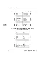
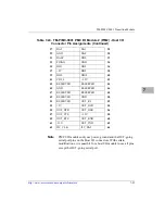
Страница 165: ...C IO13 PMC IO14 14 15 PMC IO15 PMC IO16 16 17 PMC IO17 PMC IO18 18 19 PMC IO19 PMC IO20 20 21 PMC IO21 PMC IO22 22 23 PMC IO23 PMC IO24 24 25 PMC IO25 PMC IO26 26 27 PMC IO27 PMC IO28 28 29 PMC IO29 PMC IO30 30 31 PMC IO31 PMC IO32 32 33 PMC IO33 PMC IO34 34 35 PMC IO35 PMC IO36 36 37 PMC IO37 PMC IO38 38 39 PMC IO39 PMC IO40 40 41 PMC IO41 PMC IO42 42 43 PMC IO43 PMC IO44 44 45 PMC IO45 PMC IO46 ...

Страница 166: ... is defined entirely by the PMC residing on the host A host I O module does not use any pins on this connector 55 PMC IO55 PMC IO56 56 57 PMC IO57 PMC IO58 58 59 PMC IO59 PMC IO60 60 61 PMC IO61 PMC IO62 62 63 PMC IO63 PMC IO64 64 Table 7 25 PMC I O Modules 1 and 2 PIM1 and PIM2 PMC I O Connector Pin Assignments Continued ...

Страница 167: ...7 38 Computer Group Literature Center Web Site Connector Pin Assignments 7 ...

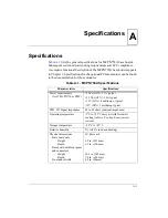
Страница 168: ...eristics Specifications Power requirements Not TMCPN710 or PMC 5Vdc 5 2 1A typical 3 3Vdc 5 2 0A typical 12V 5 4 milliamps typical 12V 5 1 milliamp typical PMC I O Signal Impedance 44 to 65 ohms nominal impedance Operating temperature 5 C to 55 C entry air with forced air cooling refer to Cooling Requirements section Storage temperature 40 C to 85 C Relative humidity 5 to 85 non condensing Physica...

Страница 169: ...l Tests were conducted with a Motorola CPX8216 system Case temperatures of critical high power density integrated circuits are monitored to ensure component vendors specifications are not exceeded The MCPN750A has been shown to operate reliably with an average air flow measurement of 355 LFM on the primary side of the board and 450 LFM on the secondary side of the board Under these circumstances a...

Страница 170: ...ded cables on all external I O ports Cable shields connected to earth ground via metal shell connectors bonded to a conductive module front panel Conductive chassis rails connected to earth ground This provides the path for connecting shields to earth ground Front panel screws properly tightened For minimum RF emissions it is essential that the conditions above be implemented Failure to do so coul...

Страница 171: ...A 4 Computer Group Literature Center Web Site Specifications A ...

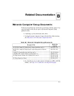
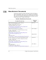
Страница 172: ...he most up to date product information in PDF or HTML format visit http www motorola com computer literature Table B 1 Motorola Computer Group Documents Document Title Publication Number MCPN750A CompactPCI Single Board Computer Installation and Use MCPN750A IH MCPN750A CompactPCI Single Board Computer Programmer s Reference Guide MCPN750A PG TMCPN710 Transition Module Installation and Use TMCPN71...

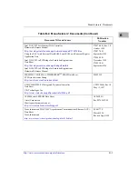
Страница 173: ...te http e www motorola com webapp DesignCenter E mail ldcformotorola hibbertco com MPC750 D MPC750TM RISC Microprocessor User s Manual Literature Distribution Center for Motorola Semiconductor Products Telephone 800 441 2447 FAX 602 994 6430 or 303 675 2150 WebSite http e www motorola com webapp DesignCenter E mail ldcformotorola hibbertco com OR IBM Microelectronics Web Site http www chips ibm co...

Страница 174: ...8 278089 001 December 1998 278091 001 September 1998 MK48T559 CMOS 8K x 8 TIMEKEEPERTM SRAM Data Sheet ST Microelectronics Group http eu st com stonline index shtml M48T559 VT82C586B PIPC PCI Integrated Peripheral Controller Data Sheet VIA Technologies Inc http www viatech com pdf productinfo 586b pdf VT82C586B Rev 1 0 May 13 1997 ATMELSerial EEPROM Data Sheet Atmel Corporation Must request docume...

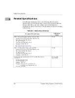
Страница 175: ...rd Specification CMC Institute of Electrical and Electronics Engineers Inc Publication and Sales Department 345 East 47th Street New York New York 10017 21633 Telephone 1 800 678 4333 http standards ieee org catalog P1386 IEEE PCI Mezzanine Card Specification PMC Institute of Electrical and Electronics Engineers Inc Publication and Sales Department 345 East 47th Street New York New York 10017 2163...

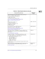
Страница 176: ...m MPR PPC RPU 02 IEEE Standard for Local Area Networks Carrier Sense Multiple Access with Collision Detection CSMA CD Access Method and Physical Layer Specifications http standards ieee org catalog IEEE 802 3 Information Technology Local and Metropolitan Networks Part 3 Carrier Sense Multiple Access with Collision Detection CSMA CD Access Method and Physical Layer Specifications Global Engineering...

Страница 177: ...CI Bridge Specification PCI ISA Specification CompactPCI Hot Swap Specification Draft PCI Industrial Manufacturers Group PICMG http www picmg com CPCI Rev 2 1 Dated 9 2 97 Rev 1 02 Rev 2 0 PICMG 2 1 DO 91 Dated 2 5 98 Table B 3 Related Specifications Continued Document Title and Source Publication Number ...

Страница 178: ... 6 8 as transition module feature 6 23 Autoboot enable 4 5 4 6 B base board layout 1 6 battery 6 14 for timer 6 11 replacing on board 6 12 battery backup on board 6 12 battery replacement 6 12 baud rate power up default 1 10 reconfiguring 1 10 BFL board failure light 6 20 big endian 2 12 block diagram MCPN750A 6 3 board configuration 1 6 board failure LED 6 20 Board Information Block hardware disp...

Страница 179: ...actPCI reset 2 11 CONADD register use 6 9 CONDAT register use 6 9 conductive chassis rails A 3 configuration logic on MCPN750A 6 8 configuration I O 1 4 1 11 1 16 configure PPC1Bug parameters 4 3 Configure Board Information Block CNFG 4 2 connector 10BaseT 100BaseT 7 12 7 22 10BaseT 100BaseT for TM PIMC 0001 7 31 for I O routing MCPN750A 7 4 connector transition for COM1 port 7 19 7 28 for COM2 po...

Страница 180: ...environmental parameters 4 1 equipment requirements for MCPN750A 1 4 ESD precautions 1 5 ethernet interface explained 6 6 Ethernet SROM caution when reading 6 6 Ethernet Station Address 6 6 Execute Code remote start 5 7 F Falcon ASIC memory controller chip set 2 3 Falcon memory controller chip set 2 9 2 12 FCC compliance A 3 firmware initialization 3 3 firmware PPCBug 3 1 Flash contents modify con...

Страница 181: ...bus 6 7 interrupt controllers for ISA interrupts 6 10 interval timers function 6 11 IOMUX PLD use of 6 8 IOMX 6 17 ISA bus 2 9 as support to M48T559 device 6 12 use 6 9 ISA DMA Channels 6 10 ISA interrupts 6 10 ISA Super I O functions 6 8 J J1 connector 7 2 Compact FLASH connector 7 31 for TM PIMC 0001 7 31 J1 connector pinouts 7 2 J10 connector for TMCPN710 7 23 J11 header for TMCPN710 7 20 J12 c...

Страница 182: ...Swap status 6 20 LEDs front panel 6 20 lithium battery replacement 6 12 little endian 2 12 M M48T559 Watchdog timer 6 15 manufacturers documents B 2 MCP750 handling big little endian 2 12 MCP750A as source of Flash memory 6 20 MCP750A described 1 1 MCP7N50A default baud rate 1 10 MCPN750 preparation 1 6 system considerations 1 10 MCPN750A debugger console port 1 10 equipment required for operation...

Страница 183: ...1 26 pin assignments connector 7 1 pinouts for J13 TMCPN710 connector 7 22 J3 MCPN750A 7 4 PMC voltage 1 21 PMC connectors 6 7 MCPN750A 7 9 PMC expansion 6 3 PMC function 6 7 PMC I O as transition module feature 6 23 PMC instal 1 21 PMC modules as I O expansion options 6 7 PMC slot 6 7 Port 92 Register as reset source 2 10 Power monitor as source of interrupt 2 9 power requirements MCPN750A 1 31 P...

Страница 184: ...up only 4 7 ROM Boot Direct Ending Address 4 7 ROM Boot Direct Starting Address 4 7 ROM Boot Enable 4 7 ROM First Access Length 4 9 SCSI Bus Reset on Debugger Startup 4 4 secondary SCSI controller 4 4 Serial Startup Code LF Enable 4 11 Serial Startup Code Master Enable 4 11 PPCBug parameters 4 1 changing 4 1 configurable by ENV 4 3 prompt debugger 3 11 PRST as reset source 2 10 push button reset 2...

Страница 185: ... chipset 2 4 software reset 2 12 sources of reset 2 9 speaker output 6 16 specifications base board A 1 stand alone operating mode jumper setting J8 1 8 startup overview 1 3 switch from one PPCBug directory to another 3 5 System Call Handler PPCBug subroutine 3 6 system clocks 2 6 system startup 2 1 T testing the hardware 3 10 timer interval 6 16 Raven 6 15 Watchdog 6 15 timers programmable 6 14 T...

Страница 186: ...s part of M48T559 6 15 as reset source 2 10 as type of interrupt 2 9 watchdog timer function 6 11 Watchdog Timer reset 2 11 Watchdog timers as part of Raven 6 15 WDT1 Raven Watchdog timer 6 15 WDT2 Raven Watchdog timer 6 15 World Wide Web address B 1 Write Read memory remote start 5 6 Write Read Virtual Register remote start 5 5 ...

Страница 187: ...Index IN 10 Computer Group Literature Center Web Site I N D E X ...

Страница 188: ...quipment Have surplus equipment taking up shelf space We ll give it a new home Learn more Visit us at artisantg com for more info on price quotes drivers technical specifications manuals and documentation Artisan Scientific Corporation dba Artisan Technology Group is not an affiliate representative or authorized distributor for any manufacturer listed herein We re here to make your life easier How...

Отзывы: