


L306 Hardware Design
Copyright © Shanghai Mobiletek Communication Ltd 42
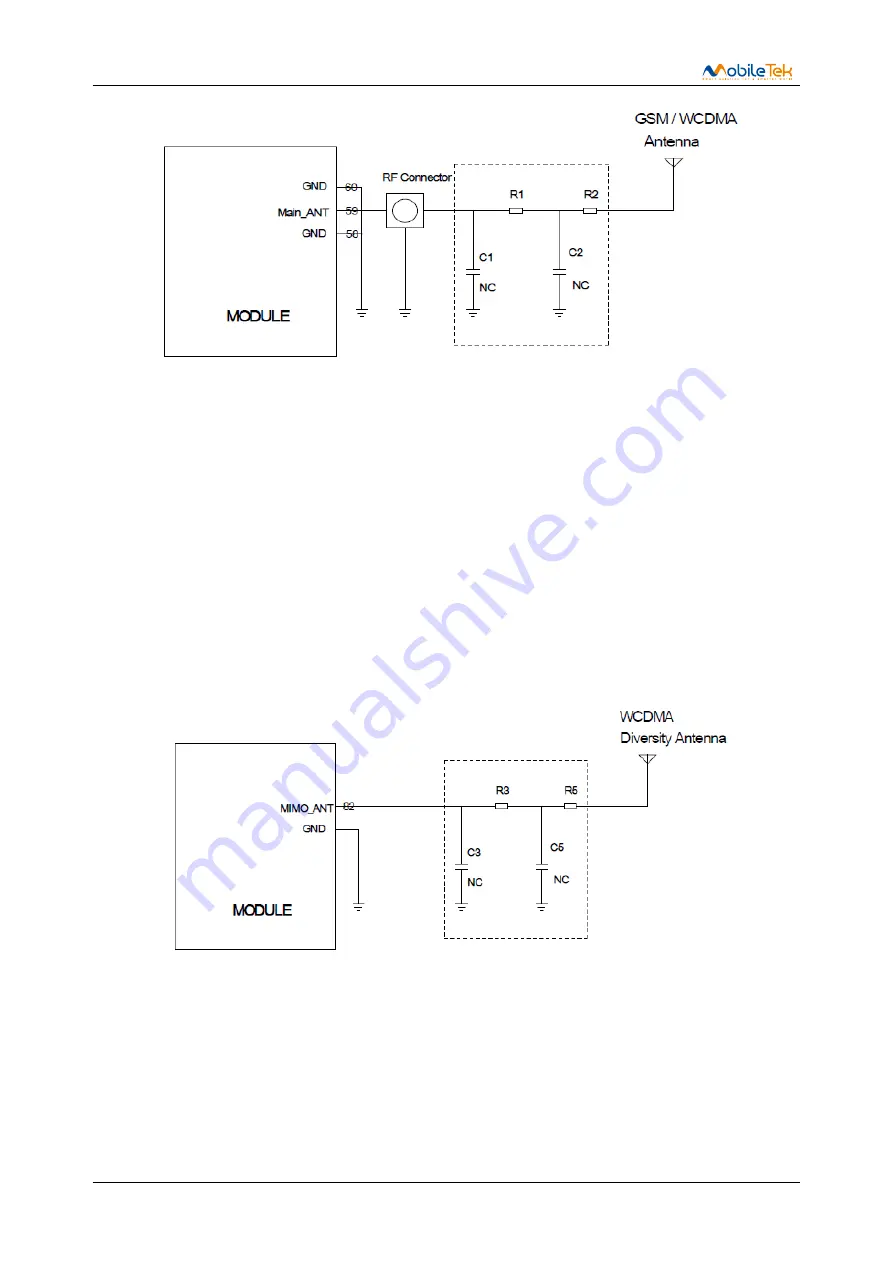
Figure 5-1 Main Antenna Design
Figure R1, C1, C2 and R2 composition of the antenna matching network for antenna debugging, the
default R1, R2 paste 0 ohm resistor C2, C1 empty paste, to be antenna factory after the antenna to
determine the value of the antenna.
Connector RF in the figure is used for testing and conducting test (for example, CE, FCC, etc.), which
need to be placed as far as possible by the module, the RF path from the module to the antenna feed
point should be kept 50 ohm impedance control.
Figure 5-2 Div Antenna Design
Figure R3, C3, C5 and R5 composition of the antenna matching network for antenna debugging, the
default R3, R5 paste 0 ohm resistor C5, C3 empty paste, to be antenna factory after the antenna to
determine the value of the antenna.
LYNQ
CONFIDENTIAL