


6-3
Figure 6-2
illustrates the Sub Sync Signal Path for
the Sub-Picture signals on the PCB-Terminal. It
functions the same as the Main Sync Signal Path
using different pin sets on the same ICs. The sub
sync signals are used by Doubler circuitry for POP/
PIP signal processing.
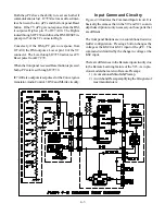
Figure 6-3
shows the sync signal functions per-
formed by the PCN-Signal. It serves to interface the
sync signals as follows:
• DVI and DM inputs to the PCB-Terminal
• Selected Main and Sub sync signals from the
Terminal to the Doubler PCBs.
• Sync from the doubler to the VCJ
The selected sync is directed to the Doubler circuitry.
If the selected source is 480i, the number of hori-
zontal lines are doubled. When the selected source
is 480p or 1080i, no line doubling is required. How-
ever, since all sync signals, 480i, 480p and 1080i
pass through the PCB-DOUBLER, the TV cannot
be operated with the PCB-DOUBLER unplugged.
IC2X10 and IC2X11 are flip-flops serving as schmitt
triggers. They effectively remove any spikes or noise
that may be riding on the sync, preventing false trig-
gering.
Содержание WS-48513
Страница 2: ......
Страница 4: ......
Страница 17: ...11 Figure 13 V23 Chassis DVI Input Block Diagram ...
Страница 21: ...1 3 Figure 1 2 Main Chassis Removal Figure 1 3 DM Replacement Step 1 Step 2 Step 3 TOP VIEW REAR VIEW TOP VIEW ...
Страница 22: ...1 4 Figure 1 4 PCB Locations Figure 1 5 Main Component Locations ...
Страница 40: ...3 10 ...
Страница 70: ...8 2 Figure 8 2 Overall Sound Circuitry Block Diagram ...
Страница 72: ...8 4 ...
Страница 75: ......
Страница 76: ...Copyright 2003 Mitsubishi Digital ElectronicsAmerica Inc 9351 Jeronimo Road Irvine CA 92618 1904 T M V23 ...


