background image

0

Development System EasydsPIC6

MikroElektronika

page

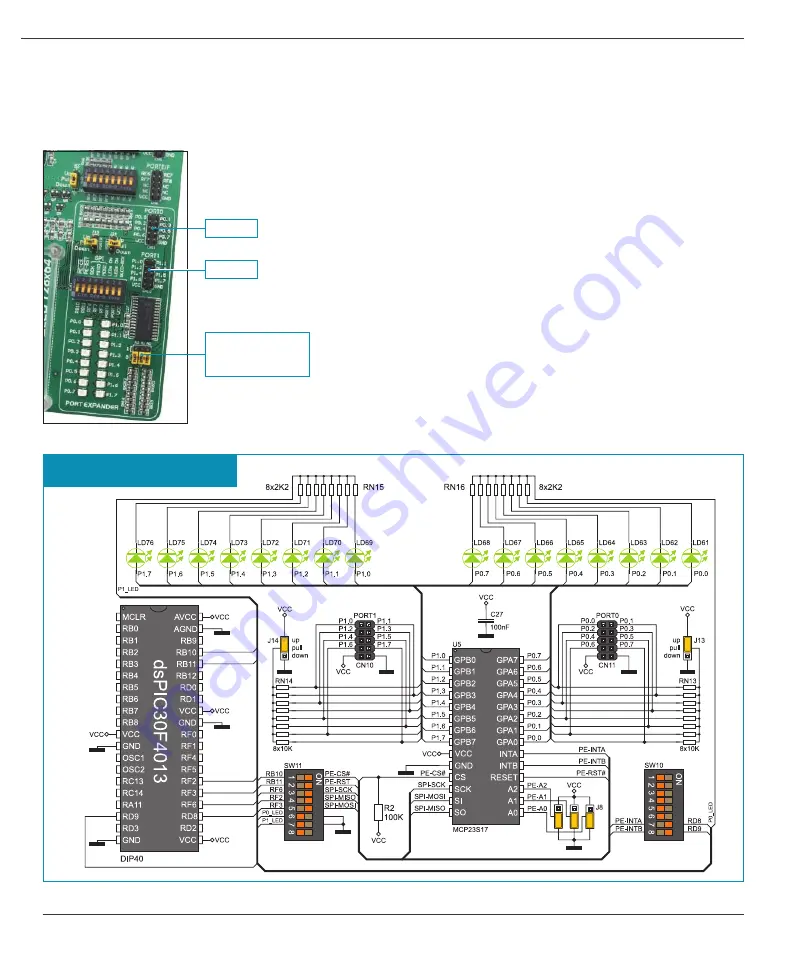
23.0. Port Expander (Additional Input/Output Ports)

SPI communication lines and MCP23S17 circuit provide the 

EasydsPIC6

 development system with means of increasing the number of 

available I/O ports by two. If the port expander communicates to the microcontroller over the DIP switch SW11 then the microcontroller 

pins RB10, RB11, RF6, RF2 and RF3 used for the operation of port expander, cannot be used as I/O pins. 

Figure 23-2

: Port expander and microcontroller connection schematic

Figure 23-1

: Port expander

PORT0

Jumper for selecting 

pull-up/pull-down  re-

sistor

The microcontroller communicates with the port expander (MCP23S17 circuit) 

using serial communication (SPI). The advantage of such communication is that 

only five lines are used for simultaneous data transceive and receive:

MOSI 

- Master Output, Slave Input (microcontroller output, MCP23S17 input)

MISO 

- Master Input, Slave Output (microcontroller input, MCP23S17 output)

SCK 

- Serial Clock (microcontroller clock signal)

CS 

- Chip Select (enables data transfer)

RST 

- Reset

Data transfer is performed in both directions simultaneously by means of MOSI and 

MISO lines. The MOSI line is used for transferring data from the microcontroller to 

the port expander, whereas the MISO line transfers data from the port expander 

to the microcontroller. The microcontroller initializes data transfer by sending a 

clock signal when the CS pin is driven low (0V). The principle of operation of the 

port expander’s ports 0 and 1 is almost identical to the operation of other ports 

on  the  development  system. The  only  difference  here  is  that  port  signals  are 

received in parallel format. The MCP23S17 converts then such signals into serial 

format and sends them to the microcontroller. The result is a reduced number of 

lines used for sending signals from ports 0 and 1 to the microcontroller. 

DIP switch SW11 enables port 

expander

PORT1

Содержание EasydsPIC6

Страница 1: ...a large number of add on modules and ready to use examples all our users regardless of their experience have the possibility to develop their project in a fast and efficient way Development System If you want to learn more about our products please visit our website at www mikroe com If you are experiencing some problems with any of our products or just need additional information please place you...

Страница 2: ...rofits and business information business interruption or any other pecuniary loss arising out of the use of this manual or product even if MikroElektronika has been advised of the possibility of such damages MikroElektronika reserves the right to change information contained in this manual at any time without prior notice if necessary HIGH RISK ACTIVITIES The products of MikroElektronika are not f...

Страница 3: ...0 ICD Connector 11 6 0 Power Supply 12 7 0 RS 232 Communication Module 13 8 0 CAN Communication Module 14 9 0 Voltage Reference Source 15 10 0 A D Converter Test Inputs 16 11 0 Serial EEPROM Module 17 12 0 DS1820 Temperature Sensor 18 13 0 Piezo Buzzer 19 14 0 LEDs 20 15 0 4x4 Keypad 21 16 0 MENU Keypad 22 17 0 Push Buttons 23 18 0 On board 2x16 LCD 24 19 0 2x16 LCD 25 20 0 128x64 Graphic LCD 26 2...

Страница 4: ...C microcontroller based devices On board USB 2 0 programmer Port expander provides an easy I O expansion by 2 additional ports In Circuit Debugger for real time debugging at hardware level Graphic LCD with backlight System specification Power Supply over an AC DC connector 7 23V AC or 9 32V DC or over a USB cable for programming 5V DC Power consumption 40mA in idle state when all on board modules ...

Страница 5: ...ctors 14 DIP switches enable pull up pull down resistors 15 Microcontroller sockets 16 Port expander 17 Potentiometer for adjusting contrast of graphic display 18 Graphic LCD connector 19 Touch panel connector 20 MENU keypad 21 4x4 keypad 22 Push buttons simulate microcontroller digital inputs 23 Jumper for selecting pins logic state via push buttons 24 Jumper for protective resistor shortening 25...

Страница 6: ...nnected to a PC When establishing a connection make sure that jumper J7 is placed in the USB position as shown in Figure 1 1 Step 3 Turn on your development system by setting the POWER SUPPLY switch to ON position Two LEDs marked as POWER and USB LINK will be automatically turned on indicating that your development system is ready to use Use the on board programmer and the dsPICprog programmer and...

Страница 7: ...g a microcontroller Figure 1 shows an unoccupied DIP40 socket Place one end of the microcontroller into the socket as shown in Figure 2 Then put the microcontroller slowly down until all the pins thereof match the socket as shown in Figure 3 Check again that everything is placed correctly and press the microcontroller easily down until it is completely plugged into the socket as shown in Figure 4 ...

Страница 8: ...n window there is a number of options for setting the operation of the microcontroller to be used A number of options which enable the programming processareprovidedontheright side of the window Positioned in the bottom right corner of the window the Progress bar enables you to monitor the programming progress 2 WriteacodeinoneofthedsPICcompilers generate a hex file and employ the on board program...

Страница 9: ...cally disconnects pins for programming from the development system In this case these pins cannot be used as I O pins When the programming process is complete the multiplexer reconnects these pins to the development system after which they can be used as I O pins Duringtheprogramming themultiplexerdisconnects the microcontroller pins used for programming from the rest of the board and connects the...

Страница 10: ...Step 2 After the Step Over command is executed the microcontroller will execute the 41st program line The next line to be executed is highlighted in blue The state of registers being changed by executing this instruction may be viewed in the Watch Values window Icon commands A list of selected registers to be monitored The state of these registers changes during the program execution which can be ...

Страница 11: ...these jumpers in the appropriate position The position of jumpers depends on the arrangement of the microcontroller pins used for programming Figures below show the position of jumpers J9 and J10 depending on which microcontroller pins are used for programming Figure 5 5 ICD connector s pinout and designations External ICD programmer is connected to RB6 and RB7 pins Figure 5 1 Pins RF2 and RF3 are...

Страница 12: ...ge of 7V to 23V or DC in the range of 9V to 32V Jumper J7 is used as a selector for a power supply source To make advantage of the USB power supply jumper J7 should be placed in the USB position When using the external power supply jumper J7 should be placed in the EXT position The development system is turned on off by switching the position of the POWER SUPPLY switch Figure 6 1 Power supply Figu...

Страница 13: ...necessary to set switches 2 RF2 and 6 RF3 on the DIP switch SW7 to ON position Which of these switches is to be used depends on which microcontroller pins are used for the USART communication Anyway the microcontroller pins used in such a communication are marked as follows RX receive data line and TX transmit data line Data rate goes up to 115 kbps In order to enable the USART module of the micro...

Страница 14: ...ion between the microcontroller and MCP2551 it is necessary to set switches 6 and 8 on the DIP switch SW8 to ON position Switches 5 and 7 on the DIP switch SW8 may also be used for this purpose Which of these switches is to be used depends solely on the arrangement of the microcontroller pins connected to CAN communication lines The RX line can be connected to the microcontroller via RF0 and RF1 p...

Страница 15: ... the voltage reference is 4 096V This voltage is suppled to the microcontroller via the RB0 pin For the RB0 pin to be fed with the reference voltage it is necessary to set switch 7 on the DIP switch SW9 to ON position Figure 9 3 Voltage reference connection schematic Figure 9 1 Voltage reference source Figure 9 2 Microcontroller pin RB0 is fed with voltage reference 4 096V voltage reference is use...

Страница 16: ...th this voltage via test inputs Jumpers J12 are used for selecting one of the following microcontroller pins RB4 RB7 to be supplied with A D conversion voltage Resistor R6 has a protective function and is used to limit current flow through the potentiometer that is to say the microcontroller pin Figure 10 1 ADC jumper s default position Figure 10 2 Pin RB4 as input pin for A D conversion Figure 10...

Страница 17: ... data and uses serial I2 C module to communicate with the microcontroller via pins RF2 and RF3 In order to enable connection between the EEPROM module and the microcontroller it is necessary to set switches 1 and 2 on the DIP switch SW9 to ON position Figure 11 2 Serial EEPROM module and microcontroller connection schematic Serial EEPROM is connected to the microcontroller via pins RF2 and RF3 Fig...

Страница 18: ...s maximum 750ms for the DS1820 to calculate temperature with a 9 bit resolution The EasydsPIC6 development system provides a separate socket for the DS1820 It may use either RA11 or RE0 pin for communication with the microcontroller which depends on switches 5 and 6 on the DIP switch SW9 Figure 12 5 switch 5 on the DIP switch SW9 is in the ON position which means that communication is performed vi...

Страница 19: ...s in the range between 20Hz and 20kHz can be used but the best performance is provided by frequencies ranging between 2kHz and 4kHz The voltage signal can be generated via microcontroller pin RB12 or RE3 whereas DIP switch SW9 is used to select which of these two pins is to be used Figure 13 2 Switch 3 on the DIP switch SW9 is in ON position piezo buzzer is connected to pin RB12 Figure 13 1 Piezo ...

Страница 20: ... current I 1mA There are 42 LEDs on the EasydsPIC6 development system which visually indicate the state of each microcontroller I O pin An active LED indicates that a logic one 1 is present on the pin In order to enable the pin state to be shown it is necessary to select appropriate port PORTB C PORTA D PORTE or PORTE F using the DIP switch SW12 Figure 14 2 LEDs and port PORTB connection schematic...

Страница 21: ...s outputs and generate a logic one 1 Pressing any button will cause a logic one 1 to be applied to input pins Push button detection is performed from within the software For example by pressing button 6 a logic one 1 will appear on the RB10 pin In order to determine which of the push buttons is pressed a logic one 1 is applied to each of the following output pins RB4 RB5 RB6 and RB7 Figure 15 3 Ke...

Страница 22: ...dditional push buttons marked as ENTER and CANCEL MENU push buttons are connected in the same way as the port PORTB push buttons Their function is determined by the user when writing the program for the microcontroller Figure 16 2 MENU keypad and microcontroller connection schematic Figure 16 1 MENU keypad Have in mind when writing program for the microcontroller that MENU keypad is connected to p...

Страница 23: ...s may shorten such resistor using jumper J11 Right next to the push buttons there is a RESET button which is used to provide the MCLR pin with the microcontroller reset signal over the on board programmer Figure 17 2 Push buttons and port PORTB connection schematic Figure 17 1 Push buttons By pressing any push button when jumper J15 is in the VCC position a logic one 5V will be applied to the appr...

Страница 24: ... communication between the port expander and the microcontroller Potentiometer P5 is used to adjust the on board display contrast Unlike 2x16 LCD the on board LCD has no backlight but similar to 2x16 LCD this display also displays digits in two lines each containing up to 16 characters of 7x5 pixels Figure 18 2 On board 2x16 LCD and microcontroller connection schematic On board programmer is conne...

Страница 25: ...lay contrast Switch 8 LCD BCK on the DIP switch SW9 is used to turn the display backlight on off Communication between this LCD and the microcontroller is performed in a 4 bit mode Alphanumeric digits are displayed in two lines each containing up to 16 characters of 7x5 pixels Figure 19 3 Alphanumeric 2x16 LCD and microcontroller connection schematic Figure 19 1 Alphanumeric LCD connector Figure 1...

Страница 26: ...her graphic content to be displayed Potentiometer P2 is used for the GLCD contrast adjustment Switch 8 GLCD BCK on the DIP switch SW11 is used to turn the display backlight on off Ports PORTB PORTD and PORTF are also used for the operation of 2x16 LCD so that these displays cannot be used simultaneously Figure 20 3 GLCD and microcontroller connection schematic Figure 20 2 GLCD connector Figure 20 ...

Страница 27: ...panel over a GLCD display Make sure that the flat cable is to the left of the GLCD as shown in Figure 4 21 0 Touch Panel The touch panel is a thin self adhesive transparent touch sensitive panel It is placed over a GLCD Its main function is to register pressure at some specific display point and to forward its coordinates in the form of analog voltage to the microcontroller Switches 5 6 7 and 8 on...

Страница 28: ...W6 each connector pin can be connected to one pull up pull down resistor Whether pins of some port are to be connected to a pull up or a pull down resistor depends on the position of jumpers J1 J6 Figure 22 4 PORTB connection schematic Figure 22 2 J4 in pull down position Figure 22 3 J4 in pull up position Jumper for pull up pull down resistor selection Figure 22 1 I O ports DIP switch to turn on ...

Страница 29: ...it is necessary to set switch 1 on the DIP switch SW3 to ON position As a result every time you press the RD0 button a logic one VCC will appear on the RD0 pin provided that jumper J15 is placed in the VCC position In order to enable port PORTD pins to be connected to pull up resistors and the port input pins to be supplied with a logic zero 0 it is necessary to place jumper J3 in the Up position ...

Страница 30: ...lave Input microcontroller output MCP23S17 input MISO Master Input Slave Output microcontroller input MCP23S17 output SCK Serial Clock microcontroller clock signal CS Chip Select enables data transfer RST Reset Data transfer is performed in both directions simultaneously by means of MOSI and MISO lines The MOSI line is used for transferring data from the microcontroller to the port expander wherea...

Страница 31: ...rofits and business information business interruption or any other pecuniary loss arising out of the use of this manual or product even if MikroElektronika has been advised of the possibility of such damages MikroElektronika reserves the right to change information contained in this manual at any time without prior notice if necessary HIGH RISK ACTIVITIES The products of MikroElektronika are not f...

Страница 32: ...a large number of add on modules and ready to use examples all our users regardless of their experience have the possibility to develop their project in a fast and efficient way Development System If you want to learn more about our products please visit our website at www mikroe com If you are experiencing some problems with any of our products or just need additional information please place you...

Страница 33: ...Mouser Electronics Authorized Distributor Click to View Pricing Inventory Delivery Lifecycle Information mikroElektronika MIKROE 472 ...

Отзывы: