


PIC16F87XA
DS39582B-page 22
2003 Microchip Technology Inc.
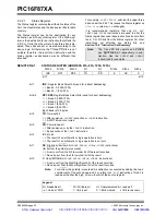
2.2.2.1
Status Register
The Status register contains the arithmetic status of the
ALU, the Reset status and the bank select bits for data
memory.
The Status register can be the destination for any
instruction, as with any other register. If the Status reg-
ister is the destination for an instruction that affects the
Z, DC or C bits, then the write to these three bits is dis-
abled. These bits are set or cleared according to the
device logic. Furthermore, the TO and PD bits are not
writable, therefore, the result of an instruction with the
Status register as destination may be different than
intended.
For example,
CLRF STATUS
, will clear the upper three
bits and set the Z bit. This leaves the Status register as
000u u1uu
(where
u
= unchanged).
It is recommended, therefore, that only
BCF
,
BSF
,
SWAPF
and
MOVWF
instructions are used to alter the
Status register because these instructions do not affect
the Z, C or DC bits from the Status register. For other
instructions not affecting any status bits, see
Section 15.0 “Instruction Set Summary”.
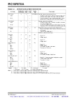
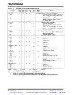
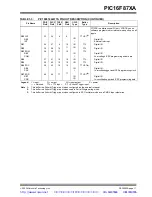
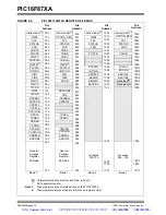
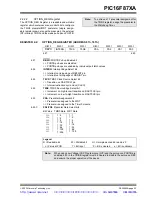
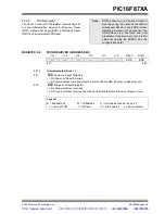
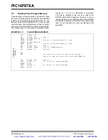
REGISTER 2-1:
STATUS REGISTER (ADDRESS 03h, 83h, 103h, 183h)
Note:
The C and DC bits operate as a borrow
and digit borrow bit, respectively, in sub-
traction. See the
SUBLW
and
SUBWF
instructions for examples.
R/W-0
R/W-0
R/W-0
R-1
R-1
R/W-x
R/W-x
R/W-x
IRP
RP1
RP0
TO
PD
Z
DC
C
bit 7
bit 0
bit 7
IRP: Register Bank Select bit (used for indirect addressing)
1
= Bank 2, 3 (100h-1FFh)
0
= Bank 0, 1 (00h-FFh)
bit 6-5
RP1:RP0: Register Bank Select bits (used for direct addressing)
11
= Bank 3 (180h-1FFh)
10
= Bank 2 (100h-17Fh)
01
= Bank 1 (80h-FFh)
00
= Bank 0 (00h-7Fh)
Each bank is 128 bytes.
bit 4
TO: Time-out bit
1
= After power-up,
CLRWDT
instruction or
SLEEP
instruction
0
= A WDT time-out occurred
bit 3
PD: Power-down bit
1
= After power-up or by the
CLRWDT
instruction
0
= By execution of the
SLEEP
instruction
bit 2
Z: Zero bit
1
= The result of an arithmetic or logic operation is zero
0
= The result of an arithmetic or logic operation is not zero
bit 1
DC: Digit carry/borrow bit (
ADDWF
,
ADDLW,SUBLW,SUBWF
instructions)
(for borrow, the polarity is reversed)
1
= A carry-out from the 4th low order bit of the result occurred
0
= No carry-out from the 4th low order bit of the result
bit 0
C: Carry/borrow bit (
ADDWF
,
ADDLW,SUBLW,SUBWF
instructions)
1
= A carry-out from the Most Significant bit of the result occurred
0
= No carry-out from the Most Significant bit of the result occurred
Note:
For borrow, the polarity is reversed. A subtraction is executed by adding the two’s
complement of the second operand. For rotate (
RRF
,
RLF
) instructions, this bit is
loaded with either the high, or low order bit of the source register.
Legend:
R = Readable bit
W = Writable bit
U = Unimplemented bit, read as ‘0’
- n = Value at POR
‘1’ = Bit is set
‘0’ = Bit is cleared
x = Bit is unknown
http://www.xinpian.net
提供单片机解密、IC解密、芯片解密业务
010-62245566 13810019655
Содержание PIC16F87XA
Страница 112: ...PIC16F87XA DS39582B page 110 2003 Microchip Technology Inc NOTES http www xinpian net IC 010 62245566 13810019655...
Страница 128: ...PIC16F87XA DS39582B page 126 2003 Microchip Technology Inc NOTES http www xinpian net IC 010 62245566 13810019655...
Страница 136: ...PIC16F87XA DS39582B page 134 2003 Microchip Technology Inc NOTES http www xinpian net IC 010 62245566 13810019655...
Страница 168: ...PIC16F87XA DS39582B page 166 2003 Microchip Technology Inc NOTES http www xinpian net IC 010 62245566 13810019655...
Страница 174: ...PIC16F87XA DS39582B page 172 2003 Microchip Technology Inc NOTES http www xinpian net IC 010 62245566 13810019655...
Страница 198: ...PIC16F87XA DS39582B page 196 2003 Microchip Technology Inc NOTES http www xinpian net IC 010 62245566 13810019655...


