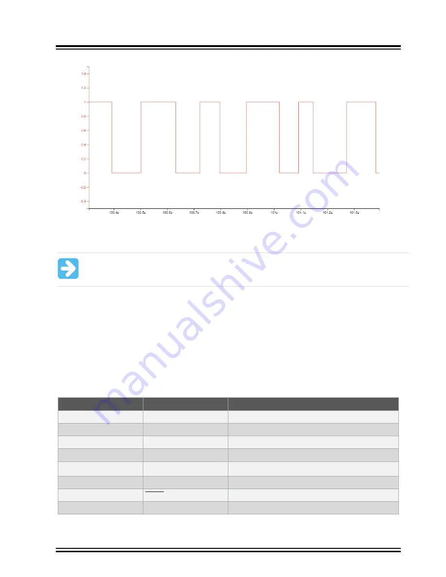
Figure 4-2. Monitoring Debug GPIO with MPLAB
®
Data Visualizer
Debug GPIO channels are timestamped, so the resolution of DGI GPIO events is determined by the resolution of the
DGI timestamp module.
Important:
Although bursts of higher-frequency signals can be captured, the useful frequency range of
signals for which debug GPIO can be used is up to about 2 kHz. Attempting to capture signals above this
frequency will result in data saturation and overflow, which may cause the DGI session to be aborted.
4.1.4.2
Timestamping
DGI sources are timestamped as they are captured by the debugger. The timestamp counter implemented in the
Curiosity Nano debugger increments at 2 MHz frequency, providing a timestamp resolution of a half microsecond.
4.2
Curiosity Nano Standard Pinout
The 12 edge connections closest to the USB connector on Curiosity Nano boards have a standardized pinout. The
program/debug pins have different functions depending on the target programming interface, as shown in the table
and figure below.
Table 4-3. Curiosity Nano Standard Pinout
Debugger Signal
Target MCU
Description
ID
—
ID line for extensions
CDC TX
UART RX
USB CDC TX line
CDC RX
UART TX
USB CDC RX line
DBG0
ICSPDAT
Debug data line
DBG1
ICSPCLK
Debug clock line
DBG2
GPIO0
debug GPIO0
DBG3
MCLR
Reset line
NC
—
No connect
PIC18F16Q40 Curiosity Nano
Curiosity Nano
©
2020 Microchip Technology Inc.
User Guide
DS50003047A-page 14


