background image


Micrel Confidential 


CENTAUR

 KS8695PX Demo Board Description

Integrated Multi-Port PCI Gateway Solution

 
The default base address for the KS8695PX system configuration registers is 0x03ff0000.  
After power up, the user is free to re-map the memory for his/her specific application.  
Here is an example of the memory space remapped for operation: 

Table 2 Memory Map Example 

Address Range 

Region Size 

Description 

0x03FF0000-0x04000000 

64 kbyte 

KS8695PX Configuration Register 
Space 

0x03E00000-0x03FEFFFF 

2 Mbyte 

Spare  

0x03A00000-0x03DFFFFF 4 

Mbyte 

External I/O bank 2 

0x03600000-0x039FFFFF 4 

Mbyte 

External I/O bank 1 

0x03200000-0x0381FFFF 4 

Mbyte 

External I/O bank 0 

0x02800000-0x031FFFFF 10 

Mbyte Space 

0x01480000-0x027FFFFF 32 

Mbyte 

FLASH 

Expansion Space 

0x01400000-0x0147FFFF 500 

kbyte 

FLASH 

0x01000000-0x013FFFFF 4 

Mbyte 

SDRAM 

Expansion Space 

0x00000000-0x00FFFFFF 16 

Mbyte SDRAM 

  
Please see the KS8695PX Detailed Register Description document for more information. 

4.1 KS8695PX 


4.1.1 Board 

Reset 

 
The KS8695PX reference board provides both a power on reset and a push button reset, 
as well as circuitry to reset the board using the Multi-ICE.  At power on, the board is 
automatically reset.  The user can also press S1, the reset button on the board for a 
manual reset.  After any reset, expect the LEDs to flash indicating the power on self test.    
 

4.1.2 System 

Clock 

 
The system clock is generated using a 25 MHz crystal (Y1).  The crystal is connected to 
the XCLK1 and XCLK2 inputs on the KS8695PX.  The clock is specified as 3.3V 
tolerant, +/- 100 ppm. 
 

4.1.3 Jumpers 

 
There are a number of jumpers and test points on the board to facilitate configuration and 
testing of the KS8695PX.  Below is a table that lists the jumpers and test points, their 
purpose, and the recommended configuration on the board. 

Содержание CENTAUR KS8695PX

Страница 1: ...iption Integrated Multi Port PCI Gateway Solution 1849 Fortune Drive San Jose CA 95131 USA Tel 408 944 0800 http www micrel com CENTAUR KS8695PX Integrated Multi Port PCI Gateway Solution Demonstratio...

Страница 2: ...AM 6 3 0 GETTING STARTED 7 3 1 CONFIGURING PC COM PORT SETTINGS 7 4 0 MEMORY MAP 8 4 1 KS8695PX ERROR BOOKMARK NOT DEFINED 4 1 1 Board Reset 9 4 1 2 System Clock 9 4 1 3 Jumpers 9 4 1 4 Chip Select As...

Страница 3: ...Block Diagram 6 Figure 2 COM Port Configuration 8 Figure 3 KS8695PX SDRAM Interface 11 Figure 4 KS8695PX Flash Interface 13 Figure 5 KS8695PX MiniPCI Interface 14 Table 1 Default Memory Map 8 Table 2...

Страница 4: ...crel Confidential 4 CENTAUR KS8695PX Demo Board Description Integrated Multi Port PCI Gateway Solution 1 0 General Information 1 1 Revision History Revision Date Description 1 0 9 26 03 Initial Releas...

Страница 5: ...are support for a mini PCI connector to address the 802 11a b g wireless gateway router market as well as a host of other applications that take advantage of the multitude of devices that connect to P...

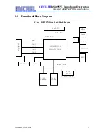
Страница 6: ...teway Solution 2 0 Functional Block Diagram Figure 1 KS8695PX Demo Board Block Diagram CENTAUR GPIO Memory Bus 16 MB STATUS LED 1 8 V MiniPCI0 16 MB PCI BUS 4 MB Et he rn et LAN3 UART LAN2 WAN KS8695P...

Страница 7: ...when the reset button on the board is depressed you should see a flashing LED pattern This is the power on self test POST 2 The ports on the KS8695PX board are labeled as WAN and LAN Connect a PC to...

Страница 8: ...Configuration 4 0 Memory Map Upon power up the KS8695PX memory map is configured as shown below Table 1 Default Memory Map Address Range Region Size Description 0x03FF0000 0x04000000 64 kbytes KS8695...

Страница 9: ...H 0x01000000 0x013FFFFF 4 Mbyte SDRAM Expansion Space 0x00000000 0x00FFFFFF 16 Mbyte SDRAM Please see the KS8695PX Detailed Register Description document for more information 4 1 KS8695PX 4 1 1 Board...

Страница 10: ...nnection for normal operation No Connection M66EN JP9 PCI 66 MHz Enable Not available on this board 0 33 MHz for this board to operate GPIO 11 6 JP5 GPIO test points for testing No connection 4 1 4 Ch...

Страница 11: ...in a 4Mx32 bit configuration The KS8695PX provides a glueless interface to the SDRAM as shown in Figure 2 The SDRAM interface can also be programmed to support 16 bit SDRAM Figure 3 KS8695PX SDRAM Int...

Страница 12: ...back from SDOCLK KS8695PX uses this clock to register SDRAM data DATA 31 0 DQ 31 0 Bi directional data bus ADDR 11 0 A 11 0 Address bus ADDR 21 20 BA 1 0 Bank Address Inputs SDCSN0 CS Chip 0 SDRAM chi...

Страница 13: ...al static memory bank 0 The KS8695PX flash data bus width is programmable for 8 16 or 32 bits The system addressing is determined by the WLED 1 0 B0SIZE 1 0 inputs The KS8695PX will automatically adju...

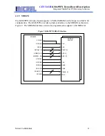
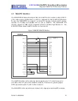
Страница 14: ...33 MHz and is compliant with PCI Local Bus Specification 2 1 The KS8695PX Demo Board miniPCI interface is shown below Figure 5 KS8695PX MiniPCI Interface KS8695P 32 4 PAD 31 0 CBEN 3 0 PAR FRAMEN TRDY...

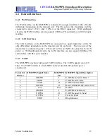
Страница 15: ...fferential termination on the transmit side for each port The line side of the transformer is connected to pins 3 TX and 6 TX on the RJ 45 connectors for LAN ports 1 4 With additional circuitry the LA...

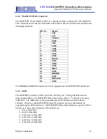
Страница 16: ...D 19 DBGACK 20 GND The DBGRQ and DBACK signals are not be supported on the KS8695PX Demo Board 4 4 5 LEDs The KS8695PX provides 2 LED s per LAN or WAN port These LED indicators are fully programmable...

Страница 17: ...through a 5 0 V DC power jack The dc power is then translated down to the voltage levels required with Micrel voltage regulators These voltage regulators were chosen for stability in evaluation and t...

Отзывы: