background image

8I20   31

REFERENCE INFORMATION

SSLBP

DATA REGISTER

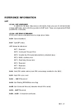
SSLBP has a global 8 bit data register for debug and custom setup  purposes. This

register allows access to internal SSLBP parameters. The data register is right justified in
the 32 bit Hostmot2 register.

LOCAL READ OPERATIONS

The sequence used for reading a local SSLBP variable is as follows: 

1. The parameter address ORed with the Request bit (bit 13) is written to the command
register.

2. The host polls the command register until it reads as zero.

3. The host reads the parameter byte from the data register

LOCAL WRITE OPERATIONS

The sequence used for writing a local SSLBP variable is as follows: 

1. The host polls the command register until it reads as zero.

2. The host writes the data byte to the data register

3. The host writes the command register with the the parameter address Ored with both
the Request bit (bit 13) and the Write bit (bit 15)

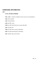
NORMAL START

When  the  FPGA  is  first  configured  or  after  a  STOP  command,  all  local

communication, error and status parameters are initialized and all LBP communication
channels are idle. A normal START command begins to establish communications with
all remote LBP devices. A normal start command is issued by writing a Start bit  with type
bits of 0,0,1 with a bit mask of the desired channels to start in the low byte (0x9NN) to the
command register. Once a start command has been issued, all channels that are selected
in the bit mask  will be probed to determine if a LBP device exists. If a device exists on a
channel,  the  SSLBP  firmware  will  acquire  the  device  type  and  device  unit  ID  from  the
remote device. When the command completes (the command register is clear), the data
register  can  be  read  to  determine  if  all  selected  channels  have  started.  A  1  bit  in  any
position in the data register indicates that the corresponding channel has failed to start. If
a  channel has failed to start, more information about the failure can be determined by
reading the CS register.

Содержание 8I20

Страница 1: ...8I20 THREE PHASE MOTOR DRIVE MANUAL V1 9 ...

Страница 2: ...AL CONTACT TO THE 8I20 CARD 1 DISCONNECT MOTOR POWER AT THE 8I20 2 DISCONNECT MOTOR U V W AT AT THE 8I20 EVEN WITH NO POWER APPLIED TO THE 8I20 A SPINNING SERVO MOTOR CAN GENERATE LETHAL VOLTAGES 3 WAIT 5 MINUTES FOR ON CARD MOTOR POWER CAPACITORS TO DISCHARGE WHEN TESTING THE 8I20 ON THE BENCH IT IS SUGGESTED TO AT THE MINIMUM 1 CONNECT THE 8I20 S CHASSIS GROUND CONNECTION TO A SECURE BUILDING GR...

Страница 3: ...FAULT CONNECTOR 4 RS 422 SERIAL CONNECTOR 5 OPERATION 6 LOGIC POWER 6 MOTOR POWER 6 MOTOR BRAKE 6 MOTOR CONNECTIONS 7 ENABLE INPUT 7 FAULT OUTPUT 7 FAULT CONDITIONS 7 CLEARING FAULTS 8 FAULT MASK 8 STATUS REGISTER 9 STATUS LEDS 10 HEATSINKING 10 DRIVE PARAMETER SETUP 11 PC HOST ADAPTER 11 SETUP COMMUNICATION WITH 8I20 12 WPD 12 RPD 13 MAIN DRIVE SETUP PARAMETERS 13 MAXCURRENT 13 BRAKEONV and BRAKE...

Страница 4: ... 24 EXAMPLE RPC COMMAND LIST 25 CRC 26 8I20 PARAMETERS LIST 27 SSLBP 30 GENERAL 30 REGISTER MAP 30 PROCESSOR INTERFACE REGISTERS 30 COMMAND REGISTER 30 DATA REGISTER 31 LOCAL READ OPERATIONS 31 LOCAL WRITE OPERATIONS 31 NORMAL START 32 8I20 DEVICE SPECIFIC SETUP 32 STOP LBP INTERFACE 32 STOP INDIVIDUAL CHANNELS 32 DOIT 32 INTERFACE REGISTERS 33 CS REGISTER 33 INTERFACE REGISTER 0 34 8I20 SPECIFIC ...

Страница 5: ...rial protocol over isolated RS 422 link Link speed allows up to 5 KHz update rates from host High side over current sensing protects the IGBT module from line line and line ground faults A brake output capable of 15A drive is provided The brake output can be driven at a presettable overvoltage setting Even though it uses a 40 MIPs DSP the 8I20 is a dumb amplifier suitable for integration in host b...

Страница 6: ...motor drive circuits are disabled In the operate mode the baud rate is set to 2 5 Mbaud default and the motor drive circuitry is enabled Setup mode is enabled to allow normal PC serial ports or USB serial adaptors to communicate with the 8I20 for setup purposes W6 controls the setup normal mode selection W6 MODE BAUD RATE UP Operate mode 2 5 Mbps default can be changed DOWN Setup Mode 115 2 Kbps f...

Страница 7: ...8I20 3 CONNECTORS 8I20 CONNECTOR LOCATIONS AND DEFAULT JUMPER POSITIONS ...

Страница 8: ...ions are 1 Chassis Gnd 2 Brake resistor 3 Brake resistor 4 Motor power 5 Motor power 6 Motor W 7 Motor V 8 Motor U 9 Chassis Gnd LOGIC POWER FAULT CONNECTOR TB1 is the logic power fault output enable input connector TB1 is a six terminal 3 5 mm pluggable screw terminal block TB1 pinout is as follows 1 Unregulated logic power 2 Unregulated Logic power 3 Enable in 4 Enable in 5 Fault out 6 Fault out...

Страница 9: ...5 Ethernet cables J1 pinout is as follows 1 RXA 2 RXB 3 TXA 4 GND 5 GND 6 TXB 7 5V 8 5V J1s pinout is designed to match breakout cards like the 7I44 A standard CAT5 or CAT5E cable can be used to connect the 8I20 to a 7I44 CAT5E cable is suggested if the serial cable is used for powering the 8I20 as the larger wire size result in lower voltage drop ...

Страница 10: ...overvoltage fault The 8I20 has local high frequency bypassing but relies on the power supplies output capacitors to supply dc power with less than 15 ripple The 8I20 also relies on power supply output capacitors to store motor inductive energy For this reason power should not be disconnected from the 8I20 power input terminals when in operation The 8I20 motor power leads should use 18 GA wire and ...

Страница 11: ... to enable motor drive If enable input is not driven the 8I20 will go into a fault state and turn off motor PWM FAULT OUTPUT The fault output is an isolated transistor OPTO coupler output The fault output is off in non masked fault conditions and on in normal operation The fault output can supply a maximum of 5 mA of output current and will switch voltages up to 24 VDC Normally the fault outputs o...

Страница 12: ...ODULEFAULT 11 Module over temperature or low gate voltage OERRFAULT 14 8I20 serial port overrun error FERRFAULT 15 8I20 serial port framing error CLEARING FAULTS Faults can not be cleared by writing the fault register but are cleared by setting the CLEARFAULT flag The host must then poll the state of CLEARFAULT until it is zero FAULT MASK Certain faults can be masked so that they do not affect the...

Страница 13: ...ble due to 8I20 temperature current limiting BRAKESTATUS 1 Current brake on status BRAKEWASONSTATUS 2 Brake has been applied status sticky WDTO 4 DSP startup due to Hardware watchdog timeout sticky SWR 5 DSP startup due to software reset sticky EXTR 6 DSP startup due to external reset sticky Sticky status bits remember events until low side power is removed or the status register is cleared ...

Страница 14: ...ipate up to 65W Heatsink thermal resistance should be chosen to keep the module temperature below 100C For example in a 50C ambient environment and continuous 2 2KW load keeping the module temperature below 100C with 65W of power dissipation requires a total thermal resistance of 100 50 65 0 77 C W The 8I20s mounting plate adds to the thermal resistance Two styles of 8I20 mounting plates are avail...

Страница 15: ...signals from a 9 pin PC serial port or USB RS 232 adapter to the 8I20s RS 422 signals via a one ended CAT5 cable A single resistor between RS 232 TXD and RS 422 RXB is needed to prevent overloading the RS 232 TXD output CAT5 PIN DE 9F PIN CAT5 SIGNAL DE 9F SIGNAL CAT5 COLOR 1 5 RXA GND ORANGE WHITE 2 3 RXB 1 TXD 1 ORANGE 3 XX TXA XX GREEN WHITE 4 5 GND GND BLUE 5 5 GND GND BLUE WHITE 6 2 TXB RXD G...

Страница 16: ...t have logic power normally supplied via TB1 2 Setup jumper must be in SETUP position DOWN 3 A RS 422 adapter must connect from the PCs serial port USB serial adapter to the 8I20 This adapter is available from Mesa 3I21 3I22 or home made adapter shown above 4 The parameter read and write programs are simple command line utilities that require some environment variables to be set before use SET COM...

Страница 17: ...e MAXCURRENT parameter sets the full scale RMS motor current of the 8I20 This is the single most important setup parameter needed to match the 8I20 to a specific motor This should be set to the maximum RMS motor current value or to 30A if the motor has a higher than 30 A RMS current rating Current torque commands are signed 16 bit numbers sent to the 8I20 and scaled such that RMS motor current QIS...

Страница 18: ...EONV and BRAKEOFFV are specified in units of 10mV That is a BRAKEONV value of 30000 would specify 300 0 V The startup values of BRAKEONV and BRAKEOFFV are set with the parameters NVBRAKEONV and NVBRAKEOFFV For example WPD NVBRAKEONV 19000 WPD NVBRAKEOFFV 17000 Would be suitable values for a 120V line operated supply with a maximum rating of 200V Note that like all EEPROM parameters these settings ...

Страница 19: ...ntegral terms Normally KQP should equal KDP and KQI should equal KDI The Startup values of KQP KDP KQI and KDI are set by the cooresponding EEPROM parameters NVKQP NVKDP NVKQI and NVKDI Default values forNV KQP and NVKDP are 50 and default values for NVKQI and NVKDI are 150000 These defaults are suitable for a large range of motors but may need to be changed to optimize current loop operation for ...

Страница 20: ...nd torque update rates to 5KHz With the default configuration the Hostmot2 interface sends referenceangle ANGLE parameter and current QSETPOINT parameter commands and receives bus voltage BUSV parameter 8I20 card temperature TEMPERATURE parameter and 8I20 status and fault information STATUS and FAULT parametera A complete host based controller will also need position sensing This may consist of qu...

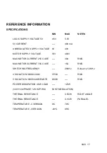
Страница 21: ...RRENT 25C CASE 30A RMS MAX MOTOR CURRENT 70C CASE 15A RMS SWITCHING FREQUENCY 20KHz Default is 12 KHz V ISOLATION VBUS LOGIC 3750V RMS V ISOLATION VBUS CASE EARTH 2500V RMS POWER DISSIPATION 4 KW LOAD 125W 340V 10A PHASE 12 KHZ PWM 60 HZ MODULATION THERMAL RESISTANCE 0 5C W RIGHT ANGLE THERMAL RESISTANCE 0 1C W PARALLEL TEMPERATURE C VERSION 0o C 70o C TEMPERATURE I VERSION 40o C 85o C ...

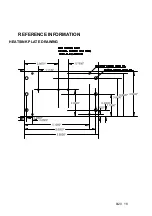
Страница 22: ...8I20 18 REFERENCE INFORMATION HEATSINK PLATE DRAWING ...

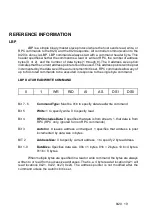
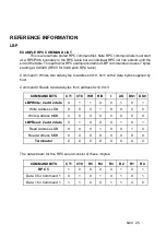
Страница 23: ...o the single byte command LBP DATA READ WRITE COMMAND 0 1 WR RID AI AS DS1 DS0 Bit 7 6 CommandType Must be 01b to specify data read write command Bit 5 Write 1 to specify write 0 to specify read Bit 4 RPCIncludesData 0 specifies that data is from stream 1 that data is from RPC RPC only ignored for non RPC commands Bit 3 AutoInc 0 leaves address unchanged 1 specifies that address is post incremente...

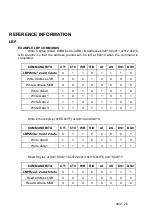
Страница 24: ... Address MSB 0 0 0 0 0 0 0 0 Write data 0 1 0 1 0 1 0 1 0 Write Data 1 1 0 1 1 1 0 1 1 Write Data 2 1 1 0 0 1 1 0 0 Write Data 3 1 1 0 1 1 1 0 1 Write 2 more bytes 0xEE 0xFF at 0x014 and 0x015 COMMAND BITS CT1 CT0 WR RID AI AS DS1 DS0 LBPWrite 0 add 2 data 0 1 1 0 0 0 0 1 Write data 0 1 1 1 0 1 1 1 0 Write data 1 1 1 1 1 1 1 1 1 Read 8 bytes at 0x010 0x011 0x012 0x013 0x014 0x015 0x016 0x017 COMMA...

Страница 25: ...Get unit address 0xC1 Get LBP status LBP Status bit definitions BIT 7 Reserved BIT 6 Command Timeout Error BIT 5 Invalid write Error attempted write to protected area BIT 4 Buffer overflow error BIT 3 Watchdog timeout error BIT 2 Reserved BIT 1 Reserved BIT 0 CRC error 0xC2 Get CRC enable status note CRCs are always enabled on the 8I20 0xC3 Get CRC error count 0xC4 0xC9 Reserved 0xCA Get Enable_RP...

Страница 26: ...guration name only on some configurations 0xD8 Get low address 0xD9 Get high address 0xDA Get LBP version 0xDB Get LBP Unit ID Serial only not used with USB 0xDC Get RPC Pitch 0xDD Get RPC SizeL Low byte of RPCSize 0xDE Get RPC SizeH High byte of RPCSize 0xDF Get LBP cookie returns 0x5A ...

Страница 27: ...RC error count 0xE4 0xE9 Reserved 0xEA Set Enable_RPCMEM access flag non zero to enable access to RPC memory 0xEB Set Command timeout in mS for USB and character times for serial 0xEC 0xEF Reserved 0xF0 0xF6 Reserved 0xF7 Write LEDs 0xF8 Set low address 0xF9 Set high address 0xFA Add byte to current address 0xFB 0xFC Reserved 0xFD Set unit ID serial only 0xFE Reset LBP processor if followed by 0x5...

Страница 28: ...CNumber Specifies RPC 0 through 63 In the 8I20 LBP implementation RPCPitch is 0x8 bytes so each RPC command has native size of 0x08 bytes and start 0x8 byte boundaries in the RPC table area RPCs can cross RPCPitch boundaries if larger than RPCPitch RPCs are needed The stored RPC commands consist of LBP headers and addresses and possibly data if the command header has the RID bit set RPC command li...

Страница 29: ...bytes to address 0x10 0x11 with 2 data bytes supplied by host Command2 Reads two data bytes from address 0x12 0x13 COMMAND BITS CT1 CT0 WR RID I AS DS1 DS0 LBPWrite 2 add 2 data 0 1 1 0 0 1 0 1 Write Address LSB 0 0 0 1 0 0 0 0 Write Address MSB 0 0 0 0 0 0 0 0 LBPRead 2 add 2 data 0 1 0 0 0 1 0 1 Read Address LSB 0 0 0 1 0 0 1 0 Read Address MSB 0 0 0 0 0 0 0 0 Terminator 0 0 0 0 0 0 0 0 The data...

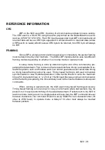
Страница 30: ...done so that relaxed interface timing is acceptable Non realtime systems such as Windows and Linux cannot guarantee exact serial data timing so timing based framing cannot be used Timing based framing is still used to maintain synchronization in case of aborted packets or noise but the timeout is set to the maximum time 25 5 character times or 2 2 mS at 115200 baud Because normal communication wil...

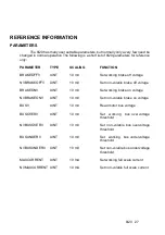
Страница 31: ...volatile brake off voltage BRAKEONV UINT 10 mV Set working brake on voltage NVBRAKEONV UINT 10 mV Set non volatile brake on voltage BUSV UINT 10 mV Read motor bus voltage BUSOVERV UINT 10 mV Set working bus overvoltage threshold NVBUSOVERV UINT 10 mV Set non volatile bus overvoltage threshold BUSUNDERV UINT 10 mV Set working bus undervoltage threshold NVBUSUNDERV UINT 10 mV Set non volatile bus un...

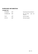
Страница 32: ...8I20 28 REFERENCE INFORMATION PARAMETERS DEADZONE UINT Set working pwm anti deadzone NVDEADZONE UINT Set non volatile pwm anti deadzone FAULT UINT 8I20 fault register STATUS UINT 8I20 status register ...

Страница 33: ...diloop I limit KQP UINT Set working qiloop p term NVKQP UINT Set non volatile qiloop p term KQI ULONG Set working qiloop I term NVKQI ULONG Set non volatile qiloop I term KQIL UINT Set working qiloop I limit NVKQIL UINT Set non volatile qiloop I limit DSETPOINT INT Set Direct current QSETPOINT INT Set Quadrature current ANGLE UINT 2 PI 65536 Set reference angle 65536 360 electrical degrees TEMPERA...

Страница 34: ...ter These registers allow low level communication to SSLBP s interface processor for issuing global commands discovery and debug operations COMMAND REGISTER The commands register is a 16 bit register right justified in the 32 bit interface with the following format W M R D S T T T N N N N N N N N W BIT 15 Write bit set high for write commands M BIT 14 ROM enable reset bit set high to reset process...

Страница 35: ...Write bit bit 15 NORMAL START When the FPGA is first configured or after a STOP command all local communication error and status parameters are initialized and all LBP communication channels are idle A normal START command begins to establish communications with all remote LBP devices A normal start command is issued by writing a Start bit with type bits of 0 0 1 with a bit mask of the desired cha...

Страница 36: ...ART command must be issued by the host to detect the changes STOP INDIVIDUAL CHANNELS In addition to stopping all channels a individual stop command can be issued A individual stop command include a bitmask of the channels to stop in the least significant 8 bits of the command DOIT In normal operation SSLBP is designed to write data from local registers to the remote device and read remote device ...

Страница 37: ...atus and control information Read access returns status information in both normal and setup mode In normal mode writes to the CS register are not used When read the CS register has the following format Byte3 Remote LBP device mode 0x80 for 8I20 0x74 for 7I64 Byte2 Communication state code debug only Byte1 Communication status code 0x00 for OK Bit 7 CommunicationNotReady Bit 6 NoRemoteID Bit 5 Com...

Страница 38: ...ted MSW Bus voltage in 10s of mV unsigned 16 bit number LSW Card Temperature in o C insigned 16 bit number Writes MSW QSETPOINT current signed 16 bit number 32767 sets current to MAXCURRENT and 32767 sets current to MAXCURRENT LSW ANGLE unsigned 16 bit number 0 to 65535 0 to 359 9945 degrees INTERFACE REGISTER 1 Interface register 1 is a general purpose 32 bit read write register for transferring ...

Страница 39: ...nterface 0 register 9 Read Interface register 0 for bus voltage and temperature note that this is stale data from previous cycle and invalid the first cycle 10 Write DOIT command 0x10NN where NN is the bit mask of channels to initiate transfers 11 Wait for next cycle at next cycle time loop to state 6 This sequence can be modified if a read modify write sequence is required but for the 8I20 the re...

Страница 40: ...nels to start 3 Wait for COMMAND register clear to verify start command completion may be many mS 4 Read data register to verify that all selected channels started a 1 bit means a fault in the channel that the bit represents 5 Write LBP word read command 0x45 in the MSByte ORed with the parameter address to the selected channels CS register 0x4500PPPP 6 Issue a DOIT Command 7 Wait for the command ...

Страница 41: ...e many mS 4 Read data register to verify that all selected channels started a 1 bit means a fault in the channel that the bit represents 5 Write the newparameter data to the selected channels Interface0 register right justified 6 Write LBP word write command 0x65 in the MSByte ORed with the parameter address to the selected channels CS register 0x6500PPPP 6 Issue a DOIT Command 7 Wait for the comm...

Отзывы: