background image

20


GX5280 User Guide


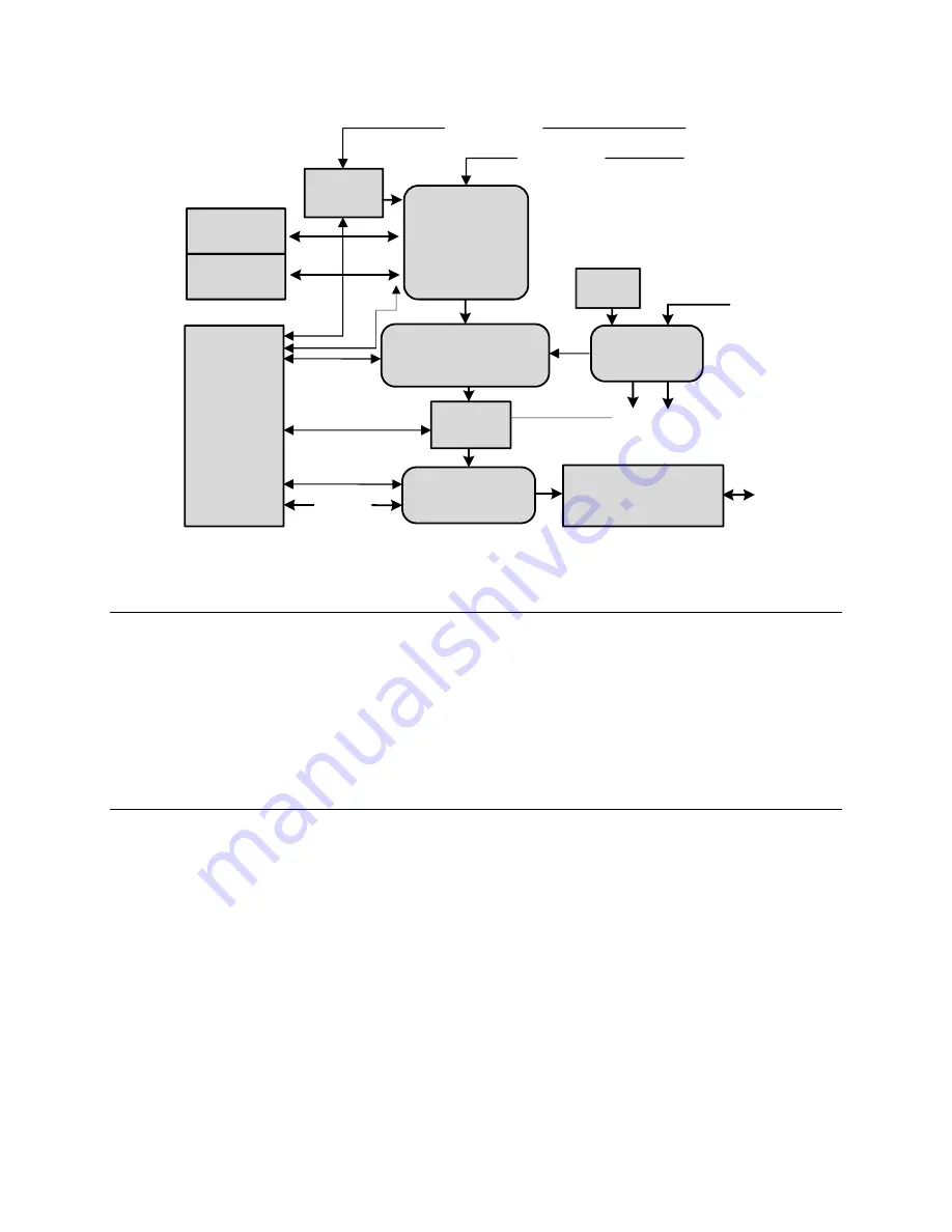
Trigger

Registers

Trigger/Pause

Logic

Run-Time Program 

Control

Counter

Registers

Programmable

Oscillator

10MHz

Data Out

Memory

Array

Output Enable

Programmable Levels

LVDS 

PXI

Interface

External

CLK

CLK STB

Trigger/Pause

External Events

PXI Trigger 

Bus

Data Bus

PXI Star 

Trigger


Figure 4-1: Architecture Diagram 

Masters and Slaves 

The DIO System (a DIO Domain) is made up of Master and Slave(s) circuit boards. The Master board can be 
connected to a maximum of 15 Slave boards expanding the number of channels in the domain. All external inputs, 
external clocks/strobes and controls are done primarily through the Master only. 

The Master distributes clock, control and status signals to all the Slaves in the domain through the PXI Bus. 

Any GX5280 board can be a Master or a Slave depends on the on-board switch settings (see Chapter 3). Although 
Master/Slave transformation can only be done when the system is shutdown. 

I/O Channels 

The operation of a GX5280 board is best understood by studying the operation of a single I/O channel.  

Figure 4-2 displays a simplified block diagram of a single I/O channel. This diagram shows how one channel 
functions.  

Содержание GX5280

Страница 1: ...GTDIO GT DIO Product Family GX5280 Dynamic Digital I O PXI Cards User s Guide Last Updated August 14 2013 ...

Страница 2: ......

Страница 3: ...sions or new versions released during the warranty period Revisions and new versions may be covered by a software support agreement If you need to return a board please contact Marvin Test Solutions Customer Technical Services Department via http www marvintest com magic the Marvin Test Solutions on line support system If You Need Help Visit our web site at http www marvintest com more information...

Страница 4: ...t Systems Inc prior company name C Builder Delphi Embarcadero Technologies Inc LabView LabWindowstm CVI National Instruments Microsoft Developer Studio Microsoft Visual C Microsoft Visual Basic NET Windows 95 98 NT ME 2000 XP VISTA Windows 7 and 8 Microsoft Corporation All other trademarks are the property of their respective owners ...

Страница 5: ...Conventions 2 Definitions 2 Chapter 2 Overview 3 Introduction 3 Computer Bus Interface 3 DIO Domains 4 GX5280 Architecture and Capabilities 5 GX5280 Models and Accessories 7 Chapter 3 Installation and Setup 9 Getting Started 9 Packing List 9 Unpacking and Inspection 10 System Requirements 10 Installation of the GTDIO Software 10 Overview of the GTDIO Software 11 Configuring Your PXI System using t...

Страница 6: ...gram Control States 26 Halt State 26 Pause State 26 Run State 26 Trigger Command 27 PC Software Trigger 27 External Trigger 27 External Trigger Control Line 27 External Event Lines 27 PXI Trigger Bus Line Trigger 28 Pause Command 28 PC Software Pause 28 External Pause 28 External Pause Control Line 28 External Pause Event Lines 29 PXI Trigger Bus Line Pause 29 Other Features of the GX5280 Board 29...

Страница 7: ...GX5280 User s Guide v J4 Control Connector 36 Appendix B Specifications 39 GX5280 DIO Specifications 39 Index 41 ...

Страница 8: ...vi GX5280 User Guide ...

Страница 9: ...tures architecture hardware and driver Chapter 3 Installation and Setup Furnishes step by step directions for installing and setting up the software and hardware Chapter 4 Theory of Operation Provides a functional hardware description Appendix A Connectors Supplies connector definitions and pin assignments Appendix B Specifications Provides a summary of the GX5280 s specifications Index Provides a...

Страница 10: ...nition DIO Digital Input Output I O DIO board Generically any of Marvin Test Solutions digital Input Output circuit boards in any board family The context could restrict it to the GX5280 family GX5280 domain A system based on GX5280 Master Slave boards These include I O Module daughter boards and associated cables and software Master board Refers specifically to the GX5280 DIO circuit board when u...

Страница 11: ... programmable dynamic Digital Input and Output I O boards These boards perform high speed automated functional testing device testing simulation and data acquisition The DIO family provides real time digital pattern capture and generation with 32 channels per card and up to 16 cards or 512 channels The DIO family uses common software development tools to develop test vector files The test vector f...

Страница 12: ...ming signals using the Master s Timing connector A full domain containing sixteen DIO boards provides up to 512 UUT I O channels 512 channels wide Because the driver supports 16 masters up to 16 domains of mixed types can in principle be supported in a PXI system The number of master slaves depends on the number of available free PXI slots in your system PXI Bus UUT Master 32 I O Slave 1 32 I O Sl...

Страница 13: ... event driven trigger generated by external events All triggers sources can work in tandem Event driven trigger can be generated by external events on the Timing connector External Event lines Event and Mask registers are used to determine both the triggering event and the masking bits to be ignored These use the D Event and D Mask registers and T Event and T Mask registers External triggering can...

Страница 14: ...ual output standards LVDS and TTL Standard 3 3V 2 5V 1 8V or 1 5V for each groups of channels when in Output mode User programmable interface input selection LVDS or TTL Standard 3 3V 2 5V 1 8V or 1 5V for each groups of channels when in Input mode User programmable PXI Star Trigger input state for Trigger and or Pause Figure 2 2 GX5280 Complete View ...

Страница 15: ... I O Board with 512 MB of vector memory and LVDS levels The following GX5280 accessories are available GT95014 Connector interface SCSI to 100 Mil Grid Single Ended I F Board GT95015 Connector interface SCSI to 100 Mil Grid Differential I F Board GT95021 2 shielded cable 68 pin SCSI GT95022 3 Shielded cable 68 pin SCSI GT95028 10 Shielded cable 68 pin SCSI GT95031 6 Shielded cable 68 pin SCSI ...

Страница 16: ...8 GX5280 User Guide ...

Страница 17: ...ge against the packing list and your purchase order and make certain all purchased items are included A DIO board package includes required items and may include options and accessories listed below Part Name Description Part Function Part Number DIO board Digital input output and domain timing and control GX5280 GTDIO software installation file GTDIO exe Installation of software driver DIOEasy ex...

Страница 18: ...configured when inserting the CD a browser will show several options select the Marvin Test Solutions Files option then locate the setup file If Auto Run is not configured you can open the Windows explorer and locate the setup files usually located under Files Setup folder You can also download the file from Marvin Test Solutions web site www MarvinTest com 2 Run the setup and follow the instructi...

Страница 19: ...is saved to PXISYS ini and PXIeSYS ini that are used by Marvin Test Solutions instruments the VISA provider and VISA based instruments drivers In addition the applet can be used to assign chassis numbers Legacy Slot numbers and instruments alias names VISA is a standard maintained by the VXI Plug Play System Alliance and the PXI Systems Alliance organizations http www vxipnp org http www pxisa org...

Страница 20: ...nds to identify your system Chassis and Controller manufacturers should provide INI and driver files for their chassis and controllers to be used by these commands 3 Change chassis numbers PXI devices Legacy Slot numbering and PXI devices Alias names These are optional steps to be performed if you would like your chassis to have different numbers Legacy slots numbers are used by older Marvin Test ...

Страница 21: ...he packing list see previous paragraph are present Electric Static Discharge ESD Precautions To reduce the risk of damage to the board the following precautions should be observed Leave the board in the anti static bags until installation requires removal The anti static bag protects the board from harmful static electricity Save the anti static bag in case the board is removed from the computer i...

Страница 22: ...elector switch designated as Master sets the Master domain that the board belongs to The adjacent selector switch designated as Slave needs to be set to 0 Slave The selector switch designated as Master sets the Master domain that the Slave board belongs to The selector switch designated as Slave select the Slave number in that domain and can be set to any number from 1 to 7 for a total of 7 Slaves...

Страница 23: ...4 to secure the module into the frame Figure 3 4 Ejector handles position after module insertion 6 Tighten the module s front panel to the chassis to secure the module in 7 Connect any necessary cables to the board 8 Plug the power cord in and turn on the PXI chassis Plug Play Driver Installation Plug Play operating systems such as Windows 9x Me Windows 2000 or XP Not Windows NT notify the user th...

Страница 24: ...n the prior section then click on the Have Disk button and browse to select the HW INF file located in C Program File Marvin Test Solutions HW If you are unable to locate the driver click Cancel to the found New Hardware wizard and exit the New Hardware Found Wizard install the DIO driver reboot your computer and repeat this procedure The Windows Device Manager open from the System applet from the...

Страница 25: ...selecting Marvin Test Solutions GTDIO DIO Panel from the Windows Start menu Initializing DIO Boards A DIO board installation is successful if the driver configuration database can be updated and all boards can be initialized When software installation is complete do the following to configure and initialize the new boards 1 Run PXI PCI Explorer from the Windows Control Panel or from the Windows St...

Страница 26: ...18 GX5280 User Guide ...

Страница 27: ...ated LVDS I O stage connector In addition the I O voltage stage can be programmed with 10 mV resolution ranges from 1 4V to 3 6V The programmed voltage level determines the logic high level for channels programmed to output mode and defines the threshold level for channels defined as input The GX5280 works as a complex programmable state machine with three main states HALT PAUSE and RUN The centra...

Страница 28: ...5 Slave boards expanding the number of channels in the domain All external inputs external clocks strobes and controls are done primarily through the Master only The Master distributes clock control and status signals to all the Slaves in the domain through the PXI Bus Any GX5280 board can be a Master or a Slave depends on the on board switch settings see Chapter 3 Although Master Slave transforma...

Страница 29: ...igh voltage level can be programmed using software see specification for details Data is going to be latched to both J1 and J2 connectors on every rising Clock when in RUN mode Channel is set to be in input mode The Channel s Direction control is set to input through software enabling the In Buffer and disables the Out Buffer The In Buffer input signal source can be programmed to be J1 or J2 input...

Страница 30: ...lable which provides a 0ns to 3ns delay in 250ps steps Together these elements provide delays in the range of 0ns to 27ns with 250ps resolution for the data out and data input clocks PXI 10 MHz External Clock J3 P31 B Clock Out J3 P20 External Strobe J3 P32 0 3nS 250pS Steps 4 7nS 250pS Steps 8 11nS 250pS Steps 12 15nS 250pS Steps 16 19nS 250pS Steps 20 23nS 250pS Steps 24 27nS 250pS Steps Clock S...

Страница 31: ...he DIO board can be driven using either internal or external clock sources In internal mode Strobe occurs Ts nanoseconds before the next clock CLK signal 8 nSec default Ts can be set from 0 24 nanoseconds before the Out CLK signal In the external mode Clock or Strobe signals are provided externally A timing diagram of the CLK and Strobe signals is shown in Figure 4 4 Clk Strobe T1 T2 TS Programmab...

Страница 32: ...ss zero and increments with the Clock Strobe signals signal towards the last memory address Vector Program Control The Vector Program Control Figure 4 6 is a high speed Event Detection with Real Time Response to those events unit controlling the program counter and the GX5280 state The inputs to the Vector Program Control are The 16 bit external events input lines or X register Trigger or Pause si...

Страница 33: ...Internal X Register Trigger Pause Logic DEvent register DMask register PEvent register PMask register TEvent register TMask register External Jump A J3 Timing Control connector Trigger External PAUSE Reset Arm Pause Halt Load Load DIO Driver External Trigger PXI Bus Trigger DIO Driver Figure 4 6 GX5280 Vector Program Control ...

Страница 34: ...are ignored following a Halt command Following Reset all I O pin channels are in the receiving mode of operation The program counter is zero the frequency is set to an internal 10MHz and the strobe timing is set to 5nSec Pause State The Vector Program Control enters a Pause state from a Halt state with an ARM command sent by the PC bus or from Run state following Pause command Run State In the Run...

Страница 35: ...ger line Pulling this line low causes the board to change its state to RUN The external trigger line overrides other trigger conditions set for the GT DIO board External Event Lines It is also possible to set a conditional trigger command which is activated upon receiving external event input lines This external event may be any expected value on all or part of the external event input lines The 1...

Страница 36: ...Bus Line can then be Enabled Disabled through software control achieving additional control over the PXI Trigger Bus event Pause Command The pause command causes the board to change its state to the Pause state and originates from the following sources PC Software External control line External events line PXI Trigger Bus Line Pause PC Software Pause The software Pause originates within the PC The...

Страница 37: ...Controlled by software the GX5280 can be programmed to Pause on any one of the PXI Trigger Bus Lines The programmed selected PXI Trigger Bus Line can then be Enabled Disabled through software control achieving additional control over the PXI Trigger Bus event Other Features of the GX5280 Board X Register The GX5280 board has a 16 bit register that can be set by software to simulate the external ev...

Страница 38: ...30 GX5280 User Guide ...

Страница 39: ...re A 1 When a GX5280 is configured as Master all connectors can be used When it configured as Slave J3 Timing and J4 Control connectors should not be used Figure A 1 GX5280 Panel Connectors for UUT Cables J2 I O LVDS Signals J4 Control Connector J1 I O TTL Signals J3 Timing Signals J2 I O LVDS Signals J4 Control Connector J1 I O TTL Signals J3 Timing Signals ...

Страница 40: ...onnector Signals J2 I O LVDS Signals LVDS I O Data Signals J3 Timing Timing Signals do not use on Slave J4 Control User Control Connector Signals do not use on Slave Note All connectors J1 J4 are 68 pin VHD connectors Figure A 2 shows the layout of 68 Pin VHD connectors The 68 pin male end plate connector has a shielded double pin row receptacle The connector mates with a UUT cable Figure A 2 GX52...

Страница 41: ... 40 GND P 57 GND P 7 IO6 I O 24 IO23 I O 41 GND P 58 GND P 8 IO7 I O 25 IO24 I O 42 GND P 59 GND P 9 IO8 I O 26 IO25 I O 43 GND P 60 GND P 10 IO9 I O 27 IO26 I O 44 GND P 61 GND P 11 IO10 I O 28 IO27 I O 45 GND P 62 GND P 12 IO11 I O 29 IO28 I O 46 GND P 63 GND P 13 IO12 I O 30 IO29 I O 47 GND P 64 GND P 14 IO13 I O 31 IO30 I O 48 GND P 65 GND P 15 IO14 I O 32 IO31 I O 49 GND P 66 GND P 16 IO15 I ...

Страница 42: ...I O 24 IO23 I O 41 IO6 I O 58 IO23 I O 8 IO7 I O 25 IO24 I O 42 IO7 I O 59 IO24 I O 9 IO8 I O 26 IO25 I O 43 IO8 I O 60 IO25 I O 10 IO9 I O 27 IO26 I O 44 IO9 I O 61 IO26 I O 11 IO10 I O 28 IO27 I O 45 IO10 I O 62 IO27 I O 12 IO11 I O 29 IO28 I O 46 IO11 I O 63 IO28 I O 13 IO12 I O 30 IO29 I O 47 IO12 I O 64 IO29 I O 14 IO13 I O 31 IO30 I O 48 IO13 I O 65 IO30 I O 15 IO14 I O 32 IO31 I O 49 IO14 I...

Страница 43: ...ut External event 7 25 GND 9 EXT8 Input External event 8 26 XTrig External Trigger Input Overrides Run Command 10 EXT9 Input External event 9 27 XPause External Pause Input Overrides Pause Command 11 EXT10 Input External event 10 28 XClkEn External Clock Enable Input 12 EXT11 Input External event 11 29 XStbEn External Strobe Enable Input 13 EXT12 Input External event 12 30 EXCLKO Output clock dist...

Страница 44: ... N C X 47 N C X 64 GND P 14 N C X 31 5V P 48 GND P 65 GND P 15 N C X 32 5V P 49 GND P 66 GND P 16 EXCLK2 X 33 VTH P 50 GND P 67 VTH P 17 EXCLK2O X 34 GND P 51 GND P 68 GND P Table A 4 68 Pin Control Connector Signals J4 Notes for Table A 4 I Input O Output P Power GND N C Reserved do not use OEN0 3n Output Enable outputs A low signal indicates output signal signals in the indicated byte group is c...

Страница 45: ...GT95014 DIO Single Ended Interface Board to User connector J4 if the LVDS clock is enabled The LVDS_N signal will get shorted to ground and device damage may result Use the GT95015 DIO Differential Interface Board for all J4 functions if the LVDS clock is required ...

Страница 46: ...38 GX5280 User Guide ...

Страница 47: ...ock Range 1 to 200MHz Resolution 0 2 Internal Strobe Phase Clock delay 0 24nS in 4nS steps Ext Test Clock 0 to 50MHz Ext Strobe 0 to 50MHz Timing skew 1nS same card 1nS between cards Clock In Direction Input into Master board Destinations Reference clock for the phase lock loop PLL Sample clock As Sample clock Frequency range 3 5 MHz to 50 MHz As Reference Clock Reference clock frequency range 10 ...

Страница 48: ...Pause As selected Override Input Trigger As selected Override Input Run As selected Indicator B Clock As selected Output Environmental Operating Temp 0 to 50 C Storage Temperature 20 to 70 C Physical Properties Bus Interface Compact PCI PXI Dimensions Single 3U Compact PCI slot PXI compatible Weight 200 gr Front Panel Connectors Label J1 I O TTL Signals type 68 pin VHD connector J2 I O LVDS Signal...

Страница 49: ... O TTL Signals 31 J1 I O TTL Signals 31 J2 I O LVDS Signals 32 Timing 33 Timing Module 33 Connectors 16 29 Conventions Style 2 D Definitions 2 Delphi i DIO Board Definition 2 Definition 2 Domain overview 4 Domain Definition 2 Overview 4 E External Event Lines 25 Pause 26 Trigger 25 External Pause 26 G GTDIO 10 GTDIO EXE 10 GX5280 Architecture and capabilities 5 GX5280 Models and Accessories 7 H Ha...

Страница 50: ... Run State 24 Run State 24 S Setup 9 10 11 Setup and Installation 9 Slave Definition 2 Slot 10 14 16 Software Pause 26 Trigger 25 Software User Guide Definition 2 Specifications 37 GX5280 37 States 24 Step Definition 2 Strobe Signals 20 Switch Settings 13 System Requirements 10 T Testware Definition 2 Theory of Operation 17 Trigger Trigger Command 25 Trigger Command 25 Trigger Command 25 V Vector ...

Отзывы: