LTC3350
30
3350fc
For more information
www.linear.com/LTC3350
applicaTions inForMaTion
The external LDO should be powered from V
OUT
. It must
be enabled after the INTV
CC
LDO has powered up and its
output must be less than 5.5V. INTV
CC
should no longer
be tied to DRV
CC
.
Minimum On-Time Considerations
Minimum on-time, t
ON(MIN)
, is the smallest time dura-
tion that the LTC3350 is capable of turning on the top
MOSFET in step-down mode. It is determined by internal
timing delays and the gate charge required to turn on the
top MOSFET. The minimum on-time for the LTC3350 is
approximately 85ns. Low duty cycle applications may
approach this minimum on-time limit and care should be
taken to ensure that:
t
ON(MIN)
<
V
CAP
V
OUT
•
f
SW
If the duty cycle falls below what can be accommodated
by the minimum on-time, the controller will begin to skip
cycles. The charge current and V
CAP
voltage will continue to
be regulated, but the ripple voltage and current will increase.
Ideal Diode MOSFET Selection
An external N-channel MOSFET is required for the input and
output ideal diodes. Important parameters for the selection
of these MOSFETs are the maximum drain-source voltage,
V
DSS
, gate threshold voltage and on-resistance (R
DS(ON)
).
When the input is grounded, either the supercapacitor stack
voltage or the step-up controller’s backup voltage is applied
across the input ideal diode MOSFET. Therefore, the V
DSS
of
the input ideal diode MOSFET must withstand the maximum
voltage on V
OUT
in backup mode. When the supercapaci-
tors are at 0V, the input voltage is applied across the output
ideal diode MOSFET. Therefore, the V
DSS
of the output ideal
diode MOSFET must withstand the highest voltage on V
IN
.
The gate drive for both ideal diodes is 5V. This allows the
use of logic-level threshold N-channel MOSFETs.
As a general rule, select MOSFETs with a low enough
R
DS(ON)
to obtain the desired V
DS
while operating at full
load current. The LTC3350 will regulate the forward voltage
drop across the input and output ideal diode MOSFETs to
30mV if R
DS(ON)
is low enough. The required R
DS(ON)
can be
calculated by dividing 0.030V by the load current in amps.
Achieving forward regulation will minimize power loss and
heat dissipation, but it is not a necessity. If a forward volt-
age drop of more than 30mV is acceptable, then a smaller
MOSFET can be used but must be sized compatible with
the higher power dissipation. Care should be taken to
ensure that the power dissipated is never allowed to rise
above the manufacturer’s recommended maximum level.
During backup mode, the output ideal diode shuts off
when the voltage on OUTFB falls below 1.3V. For high
V
OUT
backup voltages (>8.4V), the output ideal diode will
shut off when V
CAP
is more than a diode drop (~700mV)
above the V
OUT
regulation point (i.e., OUTFB > 1.2V). The
body diode of the output ideal diode N-channel MOSFET
will carry the load current until V
CAP
drops to within a
diode drop of the V
OUT
regulation voltage at which point
the synchronous controller takes over. During this period
the power dissipation in the output ideal diode MOSFET
increases significantly. Diode conduction time is small
compared to the overall backup time but can be significant
when discharging very large supercapacitors (>600F). Care
should be taken to properly heat sink the MOSFET to limit
the temperature rise.
PCB Layout Considerations
When laying out the printed circuit board, the following
guidelines should be used to ensure proper operation of
the IC. Check the following in your layout:
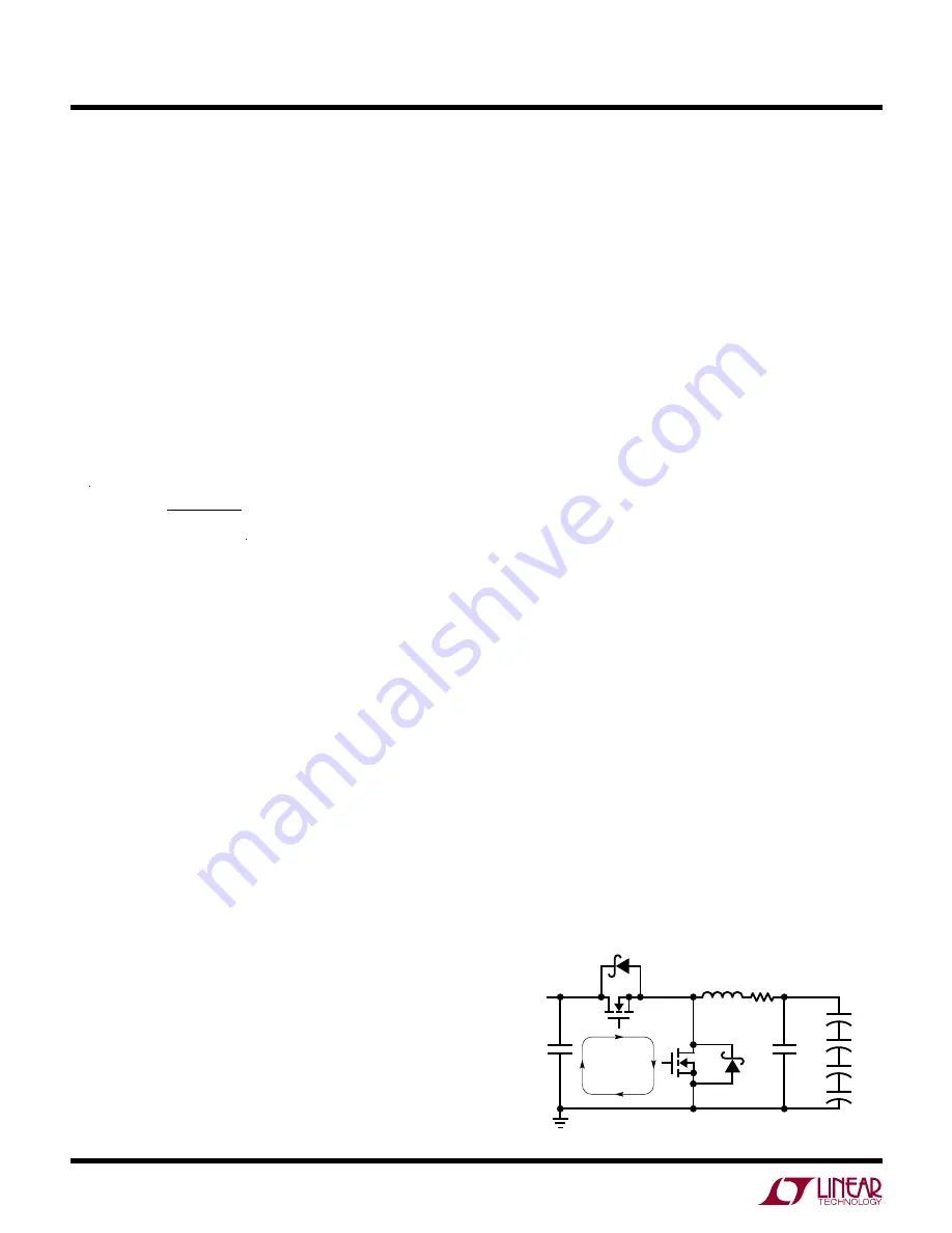
1. Keep MN1, MN2, D1, D2 and C
OUT
close together.
The high di/dt loop formed by the MOSFETs, Schottky
diodes and the V
OUT
capacitance, shown in Figure 9,
should have short, wide traces to minimize high
frequency noise and voltage stress from inductive
ringing. Surface mount components are preferred to
reduce parasitic inductances from component leads.
Figure 9. High Speed Switching Path
+
+
+
+
HIGH
FREQUENCY
CIRCULATING
PATH
MN2
MN1
V
OUT
D2
D1
C
CAP
3350 F09
C
OUT
R
SNSC
V
CAP
L1


