background image

12

LT1425

APPLICATIO

N

S I

N

FOR

M

ATIO

N

W

U

U

U

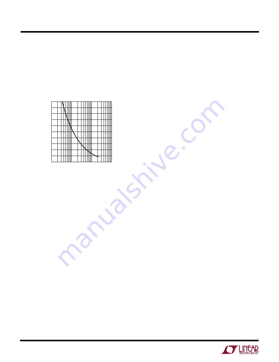
amount when output switch current is zero. Please refer
to Figure 1 which shows nominal reference current shift
at zero load for a range of R

OCOMP

 values. Example: for

a load compensation resistor of 12k, the graph indi-
cates a 1.0% shift in reference current. The R

FB

 resistor

value should be adjusted down by about 1.0% to
restore the original target output voltage.

integers, e.g., 1:1, 2:1, 3:2, etc. can be employed which
yield more freedom in setting total turns and mutual
inductance. Turns ratio can then be chosen on the basis of
desired duty cycle. However, remember that the input
supply voltage plus the secondary-to-primary referred
version of the flyback pulse (including leakage spike) must
not exceed the allowed output switch breakdown rating.

Leakage Inductance

Transformer leakage inductance (on either the primary or
secondary) causes a spike after output switch turn-off.
This is increasingly prominent at higher load currents
where more stored energy must be dissipated. In many
cases a “snubber” circuit will be required to avoid over-
voltage breakdown at the output switch node. LTC’s
Application Note 19 is a good reference on snubber
design.

In situations where the flyback pulse extends beyond the
enable delay time, the output voltage regulation will be
affected to some degree. It is important to realize that the
feedback system has a deliberately limited input range,
roughly 

±

50mV referred to the R

REF

 node, and this works

to the user’s advantage in rejecting large, i.e., higher
voltage leakage spikes. In other words, once a leakage
spike is several volts in amplitude, a further increase in
amplitude has little effect on the feedback system. So the
user is generally advised to arrange the snubber circuit to
clamp at as high a voltage as comfortably possible,
observing switch breakdown, such that leakage spike
duration is as short as possible.

As a rough guide, total leakage inductances of several
percent (of mutual inductance) or less may require a
snubber, but exhibit little to no regulation error due to
leakage spike behavior. Inductances from several percent
up to perhaps ten percent cause increasing regulation
error.

Severe leakage inductances in the double digit percentage
range should be avoided if at all possible as there is a
potential for abrupt loss of control at high load current.
This curious condition potentially occurs when the leak-
age spike becomes such a large portion of the flyback
waveform that the processing circuitry is fooled into
thinking that the leakage spike itself is the real flyback

In less critical applications, or when output current
remains relatively constant, the load compensation func-
tion may be deemed unnecessary. In such cases, a
reduced component solution may be obtained as follows:
Leave the R

OCOMP

 node open (R

OCOMP

 = 

), and replace

the filter capacitor normally on the R

CCOMP

 node with a

short to ground.

TRANSFORMER DESIGN CONSIDERATIONS

Transformer specification and design is perhaps the most
critical part of applying the LT1425 successfully. In addi-
tion to the usual list of caveats dealing with high frequency
isolated power supply transformer design, the following
information should prove useful.

Turns Ratio

Note that due to the use of an R

FB

/R

REF

 resistor ratio to set

output voltage, the user has relative freedom in selecting
transformer turns ratio to suit a given application. In other
words, “screwball” turns ratios like “1.736:1.0” can scru-
pulously be avoided! In contrast, simpler ratios of small

R

OCOMP

 (k

)

1

I

REF

 (%)

2

10

100

1000

1425 F01

1

0

Figure 1

Содержание LT1425

Страница 1: ...6W with no external power devices Byutilizingcurrentmodeswitchingtechniques it provides excellent AC and DC line regulation The LT1425 has a number of features not found on other switching regulator I...

Страница 2: ...tion 5V VIN 18V 0 01 0 04 V Voltage Gain Note 3 500 V V VIN Sense Error 10 25 mV Output Switch BV Output Switch Breakdown Voltage IC 5mA 35 50 V V VSW Output Switch ON Voltage ISW 1A 0 55 0 85 V ILIM...

Страница 3: ...Voltage vs Switch Current TEMPERATURE C 50 3 1 3 0 2 9 2 8 2 7 2 6 2 5 2 4 25 75 1425 G03 25 0 50 100 125 INPUT VOLTAGE V Switch Current Limit vs Duty Cycle Minimum Input Voltage vs Temperature SWITC...

Страница 4: ...Temperature SHDN Pin Input Current vs Voltage Minimum Synchronization Voltage vs Temperature TEMPERATURE C 50 300 295 290 285 280 275 270 265 25 75 1425 G07 25 0 50 100 125 SWITCHING FREQUENCY kHz TEM...

Страница 5: ...nd This pin is a clean ground The internal reference and feedback amplifier are referred to it Keep the ground path connection to RREF and the VC compensation capacitor free of large ground currents P...

Страница 6: ...VSW VC CEXT RFB RFB RREF RREF VBG Q4 D2 Q1 Q2 Q3 VIN I IM IM IFXD ENABLE 1425 EA LOAD COMPENSATION CURRENT AMPLIFIER DRIVER LOGIC 285kHz OSCILLATOR 2 6V REGULATOR SHDN FLYBACK ERROR AMPLIFIER COMP RCC...

Страница 7: ...tra transformer windings also exhibit defi ciencies The extra winding adds to the transformer s physical size and cost Dynamic response is often mediocre There is usually no method for maintaining loa...

Страница 8: ...n in the overall loop will then cause the voltage at the RREF resistor to be nearly equal to the bandgap reference VBG VBG is not present in final output voltage setting equation See Applications Info...

Страница 9: ...for fur ther details Enable Delay When the output switch shuts off the flyback pulse appears However it takes a finite time until the trans formerprimarysidevoltagewaveformapproximatelyrep resents th...

Страница 10: ...voltage terms in a single variable IIN K1 IOUT where K1 VOUT VIN Eff Switch current is converted to voltage by a sense resistor and amplified by the current sense amplifier with associ ated gain G Thi...

Страница 11: ...henewcompensationinplace Modify the original ROCOMP value if necessary to increase or decrease the effective compensation Once the proper load compensation resistor has been chosen it may be necessary...

Страница 12: ...m So the user is generally advised to arrange the snubber circuit to clamp at as high a voltage as comfortably possible observing switch breakdown such that leakage spike duration is as short as possi...

Страница 13: ...ble state whereby the top of the leakage spike is the control point and the trailing edge of the leakage spike triggers the collapse detect circuitry This will typically reduce the output volt age abr...

Страница 14: ...kage Inductance Leakage inductance on the transformer secondary reduces the effective primary to secondary turns ratio NP NS from its ideal value This will increase the output voltage target by a simi...

Страница 15: ...MIN where f Switching frequency nominally 285kHz LSEC Transformer secondary side inductance VOUT Output voltage tED Enable delay time tEN Minimum enable time tED tEN 2 Note that generally depending on...

Страница 16: ...se but is then held during the subsequent switch ON portion of the nextcycle ThisactionnaturallyholdstheVC voltagestable duringthecurrentcomparatorsenseaction currentmode switching PCB LAYOUT CONSIDER...

Страница 17: ...nce to discharge to 11V Feedback voltage is fed directly through a resistor divider to the RREF pin The load compensation circuitry is bypassed resulting in 5 load regulation Finally the 12V to 5V Iso...

Страница 18: ...2 F 35V 15 F 35V 3k 15 F 35V 1000pF 0 1 F 130 330pF 9 MBR0540LT1 1425 TA06 BAV21 BAV21 MUR120 LT1425 5k 18 MBR745 10 4 7 8 T1 3 2 1 GND NC RFB VC RREF SYNC SGND GND GND SHDN ROCOMP RCCOMP VIN VSW PGND...

Страница 19: ...rwise noted S Package 16 Lead Plastic Small Outline Narrow 0 150 LTC DWG 05 08 1610 0 016 0 050 0 406 1 270 0 010 0 020 0 254 0 508 45 0 8 TYP 0 008 0 010 0 203 0 254 1 2 3 4 5 6 7 8 0 150 0 157 3 810...

Страница 20: ...Flyback Regulators Uses Ultrasmall Magnetics LT1424 Application Specific Isolated Regulator 8 Pin Fixed Voltage Version of LT1425 220 F 10V 1425 TA05 LT1425 MBRS340T3 2 5 1 4 6 3 10 7 11 8 12 9 GND NC...

Отзывы: