


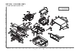


1-3
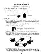
NOTES REGARDING COMPACT DISC PLAYER REPAIRS
1. Preparations
1) Compact disc players incorporate a great many ICs as well as the pick-up (laser diode). These components
are sensitive to, and easily affected by, static electricity. If such static electricity is high voltage, components
can be damaged, and for that reason components should be handled with care.
2) The pick-up is composed of many optical components and other high-precision components. Care must be
taken, therefore, to avoid repair or storage where the temperature of humidity is high, where strong
magnetism is present, or where there is excessive dust.
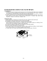
2. Notes for repair
1) Before replacing a component part, first disconnect the power supply lead wire from the unit
2) All equipment, measuring instruments and tools must be grounded.
3) The workbench should be covered with a conductive sheet and grounded.
When removing the laser pick-up from its conductive bag, do not place the pick-up on the bag. (This is
because there is the possibility of damage by static electricity.)
4) To prevent AC leakage, the metal part of the soldering iron should be grounded.
5) Workers should be grounded by an armband (1M
Ω
)
6) Care should be taken not to permit the laser pick-up to come in contact with clothing, in order to prevent
static electricity changes in the clothing to escape from the armband.
7) The laser beam from the pick-up should NEVER be directly facing the eyes or bare skin.
Содержание MBD-D102X
Страница 7: ...1 6 MEMO ...
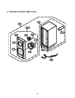
Страница 10: ...2 5 3 SPEAKER SECTION MBS D102V 750 751 752 754 755 757 A70A 758 A70 757A 759 756 753 ...
Страница 35: ...3 24 4 FOCUS WAVEFORM 1 FDO 2 F 3 F INSERT CD INSERT DVD 1 FDO 2 F 3 F ...
Страница 37: ...3 26 7 TRACKING SIGNAL 1 Tro 2 Tr 3 Tr 8 RF WAVEFORM ...
Страница 38: ...3 27 9 DISK TYPE JUGEMENT WAVEFORM 1 F 2 FDO 3 SVRRF DVD CD ...
Страница 50: ...3 39 7 MC4580 7 1 PIN CONFIGURATION 7 2 TEST CIRCUIT 7 3 ABSOLUTE MAXIMUM RATINGS TA 25 ...
Страница 60: ...3 49 3 50 WIRING DIAGRAM ...
Страница 62: ...3 53 3 54 2 MAIN FRONT BLOCK DIAGRAM ...
Страница 64: ...3 57 3 58 2 MAIN INTERFACE PWM SCHEMATIC DIAGRAM ...
Страница 65: ...3 59 3 60 3 MPEG SCHEMATIC DIAGRAM ...
Страница 66: ...3 61 3 62 4 SERVO SCHEMATIC DIAGRAM ...
Страница 67: ...3 63 3 64 5 INTERFACE SCHEMATIC DIAGRAM ...
Страница 68: ...3 65 3 66 6 FRONT SCHEMATIC DIAGRAM ...
Страница 69: ...3 67 3 68 7 FRONT MIC SCHEMATIC DIAGRAM ...
Страница 70: ...3 69 3 70 8 IPOD 1 SCHEMATIC DIAGRAM OPTION ...
Страница 71: ...3 71 3 72 9 IPOD 2 SCHEMATIC DIAGRAM OPTION ...
Страница 72: ...3 73 3 74 10 2 CHANNEL AMP SCHEMATIC DIAGRAM ...
Страница 73: ...3 75 3 76 11 BLUTHOOTH MODULE SCHEMATIC DIAGRAM OPTION ...
Страница 75: ...3 79 3 80 1 MAIN P C BOARD TOP VIEW PRINTED CIRCUIT BOARD DIAGRAMS ...
Страница 76: ...3 81 3 82 MAIN P C BOARD BOTTOM VIEW ...
Страница 77: ...3 83 3 84 2 FRONT P C BOARD TOP VIEW BOTTOM VIEW ...
Страница 78: ...3 85 3 86 3 SMPS P C BOARD TOP VIEW BOTTOM VIEW ...
Страница 79: ...3 87 3 88 MEMO 4 MIC JACK P C BOARD TOP VIEW BOTTOM VIEW 5 IPOD P C BOARD OPTION TOP VIEW BOTTOM VIEW ...