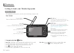
background image

- 14 -

TROUBLESHOOTING GUIDE

1. NO POWER

CHECK U801.

CHECK 

U801 PIN 1& U803 PIN

3 VOLTAGE

(5V) ?

NO

NO POWER

(POWER INDICATOR OFF)

CHECK POWER BOARD,
AND FIND OUT A SHORT
POINT AS OPENING 
EACH POWER LINE

CHECK J705 VOLTAGE 

PIN5, PIN6 (5V)?

NO

CHECK  5VR LINE
(OPEN CHECK)

CHECK 

Q803 PIN 3(3.3V) & U803

PIN 4 (1.8V)?

NO

CHECK IIC LINECONNECTION

(U501, U502)

CHECK U201 VCC, XTAL,

RESET

IS U201 

PIN88

VOLTAGE REPEATED 

AS PULSE 

SHAPE ?

NO

YES

YES

YES

NO PROBLEM

YES

CHECK KEY CONTROL

CONNECTOR ROUTINE

1

1

2

1

2

Waveforms

J705-#5, 6 / U801-#1/U803-#3

U201-#88

Содержание Flatron L1751S-BN

Страница 1: ...ding blank 1page Part No 1 2 Service Guide Specification Service Guide Specification Changes 4 REV NO MM DD YY SIGNATURE CHANGE NO CHANGE CONTENTS 1 2 3 4 5 7 6 SUFFIX LEE H J 05 04 21 L1751S S BNN L1951S S BNN LG 3828TSL082S KIM J O 05 04 21 1 Origin Notification LGEDI Printed in Indonesia LGEWA Printed in U K LGESP Printed in Brazil LGEMX Printed in Mexico LGENT Printed in China LGEIL Printed in...

Страница 2: ...t Pagination sheet P NO 3828TSL082S Total pages 28pages Cover English 2 English 3 English 4 English English Rear Cover Front cover Inside blank English English 22 English 23 English 24 English 25 Rear cover Inside 26 ...

Страница 3: ...ice com techsup html CAUTION BEFORE SERVICING THE UNIT READ THE SAFETY PRECAUTIONS IN THIS MANUAL CHASSIS NO CL 82 MODEL L1751S SN L1751S SNN AN QF L1751S BN L1751S BNN AN EF L1951S SN L1951S SNN AN QF L1951S BN L1951S BNN AN EF Same model for Service To apply the Genesis ZAN3SL Chip ...

Страница 4: ...Blank Page1 ...

Страница 5: ...min 500 Typ L1951S 3 SIGNAL Refer to the Timing Chart 3 1 Sync Signal Type Separate Sync SOG Sync On Green Composite 3 2 Video Input Signal 1 Type R G B Analog 2 Voltage Level 0 0 71 V a Color 0 0 0 Vp p b Color 7 0 0 467 Vp p c Color 15 0 0 714 Vp p 3 Input Impedance 75 Ω 3 3 Operating Frequency Horizontal 30 83kHz Vertical 56 75Hz 4 Max Resolution Analog 1280 x 1024 75Hz 5 POWER SUPPLY 5 1 Power...

Страница 6: ...e module from the ESD as it may damage the electronic circuit C MOS Make certain that treatment person s body are grounded through wrist band Do not leave the module in high temperature and in areas of high humidity for a long time The module not be exposed to the direct sunlight Avoid contact with water as it may a short circuit within the module If the surface of panel become dirty please wipe i...

Страница 7: ...st receiver ground lead to the receiver chassis ground before connecting the test receiver positive lead Always remove the test receiver ground lead last 9 Use with this receiver only the test fixtures specified in this service manual CAUTION Do not connect the test fixture ground strap to any heat sink in this receiver Electrostatically Sensitive ES Devices Some semiconductor solid state devices ...

Страница 8: ...tip as the solder melts 2 Draw away the melted solder with an anti static suction type solder removal device or with solder braid before removing the IC Replacement 1 Carefully insert the replacement IC in the circuit board 2 Carefully bend each IC lead against the circuit foil pad and solder it 3 Clean the soldered areas with a small wire bristle brush It is not necessary to reapply acrylic coati...

Страница 9: ...onnection 4 Route the jumper wire along the path of the out away copper pattern and let it overlap the previously scraped end of the good copper pattern Solder the overlapped area and clip off any excess jumper wire At Other Connections Use the following technique to repair the defective copper pattern at connections other than IC Pins This technique involves the installation of a jumper wire on t...

Страница 10: ...23 6 H Pixels 49 5 46 875 1056 800 16 80 160 800 x 600 V Lines 75 0 625 600 1 3 21 7 H Pixels 57 283 49 725 1152 832 32 64 224 832 x 624 V Lines 74 55 667 624 1 3 39 8 H Pixels 65 0 48 363 1344 1024 24 136 160 1024 x 768 V Lines 60 0 806 768 3 6 29 9 H Pixels 78 75 60 123 1312 1024 16 96 176 1024 x 768 V Lines 75 029 800 768 1 3 28 10 H Pixels 100 0 68 681 1456 1152 32 128 144 1152 x 870 V Lines 7...

Страница 11: ...crews Pell off Al tape from panel Remove the 6 screws from each up of metal frame 2 3 4 5 6 Remove Al tape from control pcb fix Remove the 4 screws from each side of metal frame 1 Pull the front cover upward 2 Then let the all latches are separated 3 Put the front face down 7 8 ...

Страница 12: ...ower Inverter BRT CTL INV CTL gmZAN3SL ADC Scaling PLL OSD LVDS Transmitter Panel MCU EEPROM System LVDS Analog R G B D Sub To Key Control 5V 3 3 V 1 8 V Regulator 3 3 V 1 8 V Switch System 5 V MOD ON 5V BLOCK DIAGRAM ...

Страница 13: ...terpolates input to 1280 X 1024 resolution signal and outputs 8 bit R G B signal to transmitter 2 Power Part This part consists of the one 3 3V regulator and one 1 8V regulator to convert power which is provided 12V 5V in Power board 5V is provided for LCD panel and Micom Also 5V is converted 3 3V by regulator and 3 3V is converted 1 8V by regulator Converted power is provided for IC in the main b...

Страница 14: ...o a DC voltage through a bridge rectifier and a bulk capacitor 3 Energy Transfer This part function is transfer the primary energy to secondary through a power transformer 4 Output rectifier and filter This part function is to make a pulse width modulation control and to provide the driver signal to power switch to adjust the duty cycle during different AC input and output loading condition to ach...

Страница 15: ... is available to LCD Monitor only 1 Port Setup a Copy UserPort sys file to c WINNT system32 drivers folder b Run Userport exe c Remove all default number d Add 300 3FF e Click Start button f Click Exit button 2 EDID Read Write 1 Run WinEDID exe 2 Edit Week of Manufacture Year of Manufacture Serial Number a Input User Info Data b Click Update button c Click Write button ...

Страница 16: ...display 2 Wait for about 5 seconds and press MENU POWER switch with 1 second interval 3 The SVC OSD menu contains additional menus that the User OSD menu as described below a Auto Color W B balance and Automatically sets the gain and offset value b NVRAM INIT EEPROM initialize 24C08 c CLEAR ETI To initialize using time d AGING Select Aging mode on off e R G B 9300K Allows you to set the R G B 9300...

Страница 17: ... POINT AS OPENING EACH POWER LINE CHECK J705 VOLTAGE PIN5 PIN6 5V NO CHECK 5VR LINE OPEN CHECK CHECK Q803 PIN 3 3 3V U803 PIN 4 1 8V NO CHECK IIC LINECONNECTION U501 U502 CHECK U201 VCC XTAL RESET IS U201 PIN88 VOLTAGE REPEATED AS PULSE SHAPE NO YES YES YES NO PROBLEM YES CHECK KEY CONTROL CONNECTOR ROUTINE 1 1 2 1 2 Waveforms J705 5 6 U801 1 U803 3 U201 88 ...

Страница 18: ...TATE 2 CHECK MICOM DIM ADJ PORT U501 PIN41 J705 PIN10 5V NO LIPS CHECK PULSE AS CONTACTING SCOPE PROBE TO CAUTION LABEL CONTACT PROBE TO CAUTION LABEL CAN YOU SEE PULSE AT YOUR SCOPE NO REPLACE CCFL LAMP IN THE LCD MODULE YES YES YES YES 3 4 Waveforms J705 9 J705 9 1 3 4 Inverter Off Micom Port check J705 Inverter output Inverter On Micom Port check J705 Inverter output 1 J705 5 6 U801 1 U803 3 ...

Страница 19: ...S 12MHZ CHECK CONNECTION LINE FROM U201 TO U501 TROUBLE IN CABLE OR LCD MODULE CHECK 5VR LINE U501 PIN8 5V YES YES YES YES 3 NO RASTER OSD IS NOT DISPLAYED gmZAN3SL NO RASTER OSD IS NOT DISPLAYED U501 PIN43 IS 64KHz H SYNC PIN44 IS 60Hz V SYNC IS PULSE APPEARED AT SIGNAL PINS NO NO NO 5 2 2 5 6 Waveforms U501 43 6 U501 44 U201 88 ...

Страница 20: ... SUB CONNECTOR LINE CHECK R G B INPUT U201 PIN 70 74 77 CHECK H SYNC LINE D SUB U501 U201 PIN95 CHECK H SYNC INPUT U201 PIN 95 YES YES YES YES CHECK V SYNC LINE D SUB U501 U201 PIN96 CHECK V SYNC INPUT U201 PIN 96 NO RASTER OSD IS DISPLAYED 4 NO RASTER OSD IS DISPLAYED gmZAN3SL TROUBLE IN LCD MODULE ...

Страница 21: ... 18 WIRING DIAGRAM Connector Ass y P N 6631T11012W or 6631T11020W Connector Ass y P N 6631T11017X L1751S 6631T11017Y L1951S Connector Ass y P N 6631T20023A or 6631T20034M ...

Страница 22: ... 19 010 020 060 070 080 090 030 100 040 050 110 EXPLODED VIEW ...

Страница 23: ...NITS SXGA LVDS 6304FLP210A LCD LIQUID CRYSTAL DISPLAY LM190E03 B4N9 LG PHILPS TFT COLOR PB FREE OF B4N2 NJ 20T TN 250NITS SXGA LVDS 3809TKL100E BACK COVER ASSEMBLY L1750S L100 PC ABS 9930 BK US VER 3809TKL101E BACK COVER ASSEMBLY L1950S L101 BRAND PC ABS 9930 BK US VER 3043TKK227G TILT SWIVEL ASSEMBLY L1750S TILT STAND BODY MX LOCAL 3043TKK227H TILT SWIVEL ASSEMBLY L1950S TILT STAND BODY MX LOCAL ...

Страница 24: ...D 16V 20 FM2 5 T C832 0CE107EF628 100UF KMG RD 16V 20 FM2 5 T C833 0CK105CD56A 1UF 1608 10V 10 R TP X7R L1951S C834 0CC102CK41A 1000PF 1608 50V 5 R TP NP0 L1951S DATE 2005 04 12 S AL LOC NO PART NO DESCRIPTION SPECIFICATION D701 0DSIH00018A ENKMC2837 T112 LF ISAHAYA R D702 0DSIH00018A ENKMC2837 T112 LF ISAHAYA R D706 0DSIH00018A ENKMC2837 T112 LF ISAHAYA R ZD701 0DZKE00138A KDZ5 6V KEC R TP USC 0 ...

Страница 25: ... 10 W 5 1608 R TP R779 0RJ0682D677 68 OHM 1 10 W 5 1608 R TP R780 0RJ2001D677 2K OHM 1 10 W 5 1608 R TP R781 0RJ2001D677 2K OHM 1 10 W 5 1608 R TP R782 0RJ0471D677 4 7 OHM 1 10 W 5 1608 R TP R803 0RJ0000D677 0 OHM 1 10 W 5 1608 R TP R805 0RJ1002D677 10K OHM 1 10 W 5 1608 R TP L1751S R806 0RJ3900D677 390 OHM 1 10 W 5 1608 R TP L1751S R807 0RJ3900D677 390 OHM 1 10 W 5 1608 R TP L1751S R809 0RJ3900D6...

Страница 26: ...SCHEMATIC DIAGRAM 23 1 SCALER L1750S L1950S ZAN3SL 1 2 U201 88 2 ...

Страница 27: ... 24 2 MICOM L1750S L1950S MICOM 2 1 5K 17 5 6 U501 43 44 5 6 ...

Страница 28: ... 25 3 POWER L1750S L1950S POWER 3 390 390 390 390 1 J707 5 6 U801 1 U803 3 1 1 ...

Страница 29: ... 4 CONNECTOR JACKS L1750S L1950S CONNECTOR JACKS 4 15K 4 J707 2 3 J707 2 1 J707 5 6 U801 1 U803 3 1 4 3 Inverter Off Micom Port check J705 Inverter output Inverter On Micom Port check J705 Inverter output ...

Страница 30: ...Apr 2005 P NO 3828TSL082S Printed in Korea ...

Отзывы: