background image

3-12

ONE POINT REPAIR GUIDE

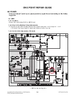
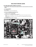
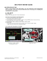
NO SOUND 

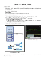
There is no sound output by DIGITAL AUDIO AMP DAMAGE, repair the set according 
to the following guide.

5-2. BY DIGITAL AUDIO AMP DAMAGE (IN ALL FUNCTIONS)

5-2-1. Solution

Please check and replace IC701, IC702 on MAIN board.

5-2-2. How to troubleshoot (Countermeasure)

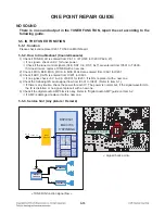
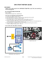
1) Check PWM_FL±, PWM_FR± & PWM_SW± signals from IC601 to IC701 & 702 each input function.



 If no signal, check if I2S audio signals are entered to IC601.

       Refer to “I2S audio signal interface” on Item 5-1.
2) Check PVDD.



 If PVDD is abnormal, check the SMPS.

3) Check +12 V for driving the gate of AMP IC.
    a. All the powers are normal, but if +12 V is low, there is possible for AMP IC to be damaged.
    b. Remove L710, L711, L712 and L713 one by one.
        When removed a inductance, if +12 V is recovered, the IC connected to it was damaged.
    c. Replace the IC with a new one.
4) Check the impedance between IC701/IC702_OUT_A/OUT_B & GND.
    a. If the impedance is 0 

Ω

, the IC must be damaged.

    b. After removing the heat sink, replace it with a new one.

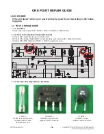
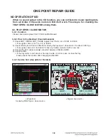
5-2-3. Service hint (Any picture / Remark)

< Signal check point >

L710

IC702

IC701

L711

L712

L713

Содержание CM4550

Страница 1: ...CAUTION BEFORE SERVICING THE UNIT READ THE SAFETY PRECAUTIONS IN THIS MANUAL SERVICE MANUAL Internal Use Only MARCH 2016 P NO AFN77483203 MODEL CM4550 CM4550 CMS4550F W MODEL CM4550 CM4550 CMS4550F W Mini Hi Fi System ...

Страница 2: ...CONTENTS SECTION 1 GENERAL SECTION 2 CABINET MAIN CHASSIS SECTION 3 ELECTRICAL SECTION 4 REPLACEMENT PARTS LIST 1 1 ...

Страница 3: ... SUMMARY CONTENTS SERVICING PRECAUTIONS 1 3 ESD PRECAUTIONS 1 5 HIDDEN KEY MODE 1 6 SERVICE INFORMATION FOR EEPROM 1 7 PROGRAM DOWNLOAD UPDATE GUIDE 1 8 1 MCS PROGRAM 1 8 2 EQ PROGRAM 1 9 SPECIFICATIONS 1 10 1 2 ...

Страница 4: ...the eyes Absolutely never permit laser beams to enter the eyes Also NEVER switch ON the power to the laser output part lens etc of the pick up if it is damaged 5 Cleaning the lens surface If there is dust on the lens surface the dust should be cleaned away by using an air bush such as used for camera lens The lens is held by a delicate spring When cleaning the lens surface therefore a cot ton swab...

Страница 5: ... replacing a component part first disconnect the power supply lead wire from the unit 2 All equipment measuring instruments and tools must be grounded 3 The workbench should be covered with a conductive sheet and grounded When removing the laser pick up from its conductive bag do not place the pick up on the bag This is because there is the possibility of damage by static electricity 4 To prevent ...

Страница 6: ... damage ESD devices 5 Do not use freon propelled chemicals These can generate electrical charges sufficient to damage ESD devices 6 Do not remove a replacement ESD device from its protective package until immediately before you are ready to install it Most replacement ESD devices are packaged with leads electrically shorted together by conductive foam aluminum foil or comparable conductive materia...

Страница 7: ...ROM Option by SKIP 3 Clear EEPROM Front Key STOP RCU Key SKIP 4 Edit EEPROM Front Key STOP RCU Key SKIP You can change the digit of option by SKIP You can edit 0 f by REPEAT or PLAY PAUSE key 5 Bluetooth DUT Front Key STOP RCU Key PROGRAM Bluetooth model only 6 Power Disc Lock On Off CD Function Only Active Front Key STOP RCU Key EQ 7 Amp Clip On Off Front Key STOP RCU Key Mute Amp Clip Mode Chang...

Страница 8: ...t STOP push same timing during 5 seconds FLD OP 0 Move to appropriate position and make changes with remote control skip mode play key Press ENTER key FLD write ok Remote control Fwd skip Front STOP push same timing FLD E2P CLR Completed 1 7 SERVICE INFORMATION FOR EEPROM ...

Страница 9: ...are then download the file to your set Caution When downloading the file you should neither unplug the USB device change to the other function nor power off the device USB device must be unplugged when the downloading process is completed ON VFD DISPLAY SCREEN NO USB Insert USB device at USB function SEARCH FIRMWARE FINISH POWER OFF MANUALLY When completed remove USB device 1 8 PROGRAM DOWNLOAD UP...

Страница 10: ...B storage device and disable the security software then download the file to your set Caution When downloading the file you should neither unplug the USB device change to the other function nor power off the device USB device must be unplugged when the downloading process is completed ON VFD DISPLAY SCREEN NO USB Insert USB device at USB function SEARCH EQ UP FINISH POWER OFF AUTOMATICALLY When co...

Страница 11: ...R FM Tuning Range 87 5 to 108 0 MHz or 87 50 to 108 00 MHz AMPLIFIER Total output 700 W Front 230 W X 2 3 Ω at 1 kHz Subwoofer 240 W 3 Ω at 1 kHz THD 20 CD Frequency Response 100 to 20 000 Hz Signal to noise ratio 75 dB Dynamic range 75 dB FRONT SPEAKER Type 2 Way 2 Speaker Impedance 3 Ω Rated Input Power 230 W Max Input power 460 W Net Dimensions W x H x D 266 x 306 x 263 mm Net Weight 3 1 kg SUB...

Страница 12: ...SECTION 2 CABINET MAIN CHASSIS CONTENTS EXPLODED VIEWS 2 3 1 CABINET AND MAIN FRAME SECTION CM4550 2 3 2 MECHANISM DECK SECTION DP17TM3 2 5 3 PACKING ACCESSORY SECTION 2 7 4 SPEAKER SECTION 2 8 2 1 ...

Страница 13: ...2 2 ...

Страница 14: ...64 A47 264 463 463 269 262 460 464 464 263 255 255 443 443 A43 443 443 A46 464 265 266 A44 266 464 261 252 A52 259 464 464 A42 251 253 CABLE1 CABLE4 300 NOTES THE EXCLAMATION POINT WITHIN AN EQUILATERAL TRIANGLE IS INTENDED TO ALERT THE SERVICE PERSONNEL TO THE PRESENCE OF IMPORTANT SAFETY INFORMATION IN SERVICE LITERATURE ...

Страница 15: ...2 MECHANISM DECK SECTION DP17TM3 1026 1439 A001 1002 1005 1001 1049 1437 1437 1024 1024 1024 A006 1016 1013 1015 1020 1024 1003 1439 1018 1019 1011 1012 1437 1004 A005 1045 1043 1030 ...

Страница 16: ...808 Battery 900 Remote Control 825 FM Wire Antenna 802 Box 801 Instruction Ass y 804 Bag 803 Packing 803 Packing 3 PACKING ACCESSORY SECTION ...

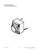
Страница 17: ...A60 4 SPEAKER SECTION 4 1 FRONT SPEAKER CMS4550F ...

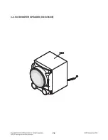
Страница 18: ...2 9 A90 4 2 SUBWOOFER SPEAKER CMS4550W ...

Страница 19: ...2 10 ...

Страница 20: ...OOTING GUIDE 3 27 1 CD FUNCTION 3 27 2 DOUBLE USB FUNCTION 3 28 WAVEFORMS OF MAJOR CHECK POINT 3 29 1 SDRAM 3 29 2 SERVO 3 29 3 AUDIO PATH 3 30 4 USB 3 31 WIRING DIAGRAM 3 33 BLOCK DIAGRAMS 3 35 1 SYSTEM BLOCK DIAGRAM 3 35 2 SMPS BLOCK DIAGRAM 3 37 3 AUDIO PATH BLOCK DIAGRAM 3 39 4 POWER DIAGRAM 3 41 CIRCUIT DIAGRAMS 3 43 1 SMPS CIRCUIT DIAGRAM 3 43 2 MAIN DSP CIRCUIT DIAGRAM 3 45 3 MAIN SERVO CIR...

Страница 21: ...ubleshoot Countermeasure 1 Check if the fuse F901 is open or short circuit 2 Check if the bridge diode BD901 is short circuit by over current with a digital multi meter 3 Check if the NTC thermistor TH901 or TH903 is normal or open 1 1 3 Service hint Any picture Remark F901 If F901 is not short circuit replace it with a same specifications one TH901 If TH901 is open replace it with a new one BD901...

Страница 22: ... 2 D951 1 2 1 Solution Please check and replace D951 on SMPS board 1 2 2 How to troubleshoot Countermeasure 1 Check the anode cathod voltage of D951 with a digital multi meter it is normally 0 2 0 3 V If it doesn t have any voltage it s destroyed Replace it with a new one 1 2 3 Service hint Any picture Remark SMPS schematic diagram ...

Страница 23: ...bleshoot Countermeasure 1 Check 5 6 V to CN501 in standby mode If there is no 5 6 V check the SMPS 2 Check 12 V F F and PVDD when power on the set If the set doesn t work regardless of what the KEY1 changes high to low while pressing the power button X500 and X501 work normally but if you can not power on the set replace IC501 with a new one on the MAIN board 2 1 3 Service hint Any picture Remark ...

Страница 24: ... Check if IC501 outputs VFD_D0 VFD_CLK and VFD_STB to the FRONT board 3 Check the GR signal pulse signal of IC408 on the FRONT board Check the SG signal pulse signal of IC408 on the FRONT board If the GR and SG signal isn t output replace IC408 with a new one If the GR and SG signal is output replace DIG302 with a new one 3 1 3 Service hint Any picture Remark GR signal SG signal Waveform of GR and...

Страница 25: ...he SPDO signal from pin24 of IC407 If no signal check 3 3 V RF and X400 2 Check the SPIN SPIN from IC408 to CN405 for driving SPINDLE motor It is about 3 6 Vp p If no signal check 1 8 V and 5 V for IC408 3 Check if the FFC cable is solidly connected between CN405 and MD 4 Check the MD If the spindle motor is sort circuit or has any trouble it can not rotate CD discs Please check the function after...

Страница 26: ...l from Pin23 of IC407 If no signal check 3 3 V RF and X400 2 Check the SLED SLED from IC408 to CN405 for driving SPINDLE motor It is about 2 9 Vp p If no signal check 1 8 V and 5 V for IC408 3 Check if the FFC cable is solidly connected between CN405 and MD 4 Check the MD If the sled motor is sort circuit or has any trouble it can not move the pickup module Please check the function after changing...

Страница 27: ...signal check 1 8 V 5 V to IC408 2 Check LOAD from IC408 to CN405 for driving the tray open close motor It is about 3 85 Vp p If no signal check 5 V to IC408 If it has any trouble replace it with a new one 3 Check if the FFC cable is solidly connected between CN405 and MD 4 Check the MD If the tray motor is sort circuit or has any trouble it can not open or close the tray Please check the function ...

Страница 28: ...beam be positioned in the center of a track on CD disc 1 Check the TRD signal from Pin22 of IC407 If no signal check 3 3 V RF and X400 2 Check TR TR from IC408 to CN408 for driving the tracking actuator If no signal check 1 8 V and 5 V for IC408 3 Check if the FFC cable is solidly connected between CN405 and MD 4 Check the MD If the pickup module has any trouble it can not move the laser beam on t...

Страница 29: ...beam keep a regular interval with the surface of a CD disc 1 Check the FOD signal from Pin21 of IC407 If no signal check 3 3 V RF and X400 2 Check F F from IC408 to CN405 for driving the focusing actuator If no signal check 1 8 V and 5 V for IC408 3 Check if the FFC cable is solidly connected between CN405 and MD 4 Check the MD If the pickup module has any trouble it can not move the laser beam on...

Страница 30: ...signal waveform to the IC is distorted or no signal replace it with a new one 3 Check if Digital audio AMP block on Item 5 2 is normal 5 1 3 Service hint Any picture Remark MCS_MCLK 16 93 MHz MCS_BCK 1 4 MHz MCS_DATA_OUT MCS_LRCK 44 1 KHz Waveform of I2S audio interface signals I2S Signal Flow M P UP PWM TAS5548 TAS5624LA FR FL Woofer 12 288 MHZ TAS5624LA IC407 LC78615E New DSPIC501 MLC3730 176PIN...

Страница 31: ...efer to I2S audio signal interface on Item 5 1 2 Check PVDD If PVDD is abnormal check the SMPS 3 Check 12 V for driving the gate of AMP IC a All the powers are normal but if 12 V is low there is possible for AMP IC to be damaged b Remove L710 L711 L712 and L713 one by one When removed a inductance if 12 V is recovered the IC connected to it was damaged c Replace the IC with a new one 4 Check the i...

Страница 32: ... distorted or no signal replace it with a new one 3 Check if Digital audio AMP block on item 5 2 is normal 5 3 3 Service hint Any picture Remark D to pin 1 4 of CN302 D to pin 2 5 of CN302 Waveform of USB D signal USB function signal flow PWM TAS5548 TAS5624LA FR FL Woofer 12 288 MHZ TAS5624LA DSPIC501 MLC3730 176PIN BGA USB1_D USB2_D Interrupt controller CDROM x8 speed Decoder NAND Controller wit...

Страница 33: ...the digital audio AMP block is okay Refer to Digital Audio AMP guide on Item 5 2 If AMP is damaged replace it with a new one 5 4 3 Service hint Any picture Remark Signal check point AUX function signal flow PWM TAS5548 TAS5624LA FR FL Woofer 12 288 MHZ TAS5624LA DSPIC501 MLC3730 176PIN BGA IC201 CS5346 AUX AUX_L R Interrupt controller CDROM x8 speed Decoder NAND Controller within BCH codec 14bits ...

Страница 34: ...power for each IC The power is normal but if the signal waveform to the IC is distorted or no signal replace it with a new one 5 Check if the digital audio AMP block is okay Refer to Digital Audio AMP guide on Item 5 2 If AMP is damaged replace it with a new one 5 5 3 Service hint Any picture Remark Signal check point TUNER IN function signal flow PWM TAS5548 TAS5624LA FR FL Woofer 12 288 MHZ TAS5...

Страница 35: ... it with a new one 5 Check if the digital audio AMP block is okay Refer to Digital Audio AMP guide on Item 5 2 If AMP is damaged replace it with a new one 5 6 3 Service hint Any picture Remark Signal check point PORTABLE function signal flow PWM TAS5548 TAS5624LA FR FL Woofer 12 288 MHZ TAS5624LA DSPIC501 MLC3730 176PIN BGA IC201 CS5346 Portable PTB_L R Interrupt controller CDROM x8 speed Decoder ...

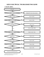
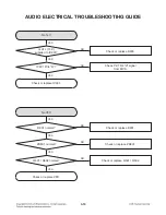
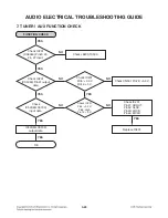
Страница 36: ...Is Vcc 10 V 18 V supplied to IC901 Pin7 D902 normal YES NO Check or replace D902 Is there about 2 5 V at IC941 Pin1 Replace IC941 YES NO D935 normal Replace D935 YES NO D932 normal Replace D932 YES NO D931 normal Replace D931 YES NO D933 D934 normal Replace D933 D934 YES NO Power line of main PCB is short NO 3 17 AUDIO ELECTRICAL TROUBLESHOOTIHG GUIDE ...

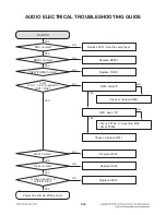
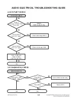
Страница 37: ... V 18 V supplied to IC911 Pin4 D903 normal YES NO Check or replace D903 Check P CTRL H signal from MCS Check PC902 Q901 normal Replace Q901 Check or replace Q911 YES NO D951 normal Replace D951 YES NO Is there about 2 5 V at IC951 Pin1 Replace IC951 YES NO Q911 base H Power line of main PCB is short NO NO 3 18 AUDIO ELECTRICAL TROUBLESHOOTIHG GUIDE ...

Страница 38: ...Pin4 H Check P CTRL H signal from MCS YES NO Check or replace IC931 No VFD D931 normal Check or replace D931 YES YES NO ZD931 normal Q501 Q502 normal Check or replace ZD931 Check or replace Q501 Q502 YES YES NO NO Check or replace VFD 3 19 AUDIO ELECTRICAL TROUBLESHOOTIHG GUIDE ...

Страница 39: ... NO Check if IC510 have 3 3 V output Check if IC508 have 1 2 V output X501 32 768 kHz X500 24 MHz Check the operation OK YES YES YES YES YES 3 IC504 M24C16 CHECK CHECK IC501 PIN Refer to MCS troubleshooting NO Check pinC2 pinB1 DATA CLK Replace MCS NO YES Check MCS voltage 3 3 VA Check MCS YES OK OK YES YES NO 3 20 AUDIO ELECTRICAL TROUBLESHOOTIHG GUIDE ...

Страница 40: ... VKK Pin8 5 6 V YES OK NO Check CN301 connection YES Check each Pin voltage YES Check IC301 MC3401 voltage Pin30 VKK 25 8 V Pin13 43 3 3 V YES Check IC501 IC301 data communication STB DATA CLK FLD light on OK NO If voltage is not 3 4 V YES Check IC301 YES NO Replace IC301 NO Check input data IC501 Pin F1 F2 G1 YES OK Check IC501 YES NO Replace IC501 Check output data IC501 Pin D2 YES YES YES 3 21 ...

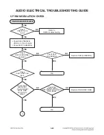
Страница 41: ... troubleshooting Check X601 12 288 MHz operation NO Replace X601 12 288 MHz Check X601 12 288 MHz OK YES NO Check IC601 Pin21 CLK input Check IC501 MLC3730 Pin B3 RESET Pin A1 SDA Pin A2 SCL output NO Replace R53E R53C R53B Check line resistor output RST R53E SCL R53C SDA R53B NO YES YES YES YES YES YES OK YES A 3 22 AUDIO ELECTRICAL TROUBLESHOOTIHG GUIDE ...

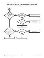
Страница 42: ...g Check CD Assy communication Pin22 23 24 OK NO NO Check each line resistor output Check IC601 input data Check PWM modulator output FL Pin48 49 FR Pin46 47 Other output check NO Replace IC601 Check IC601 NO OK YES YES YES YES YES YES A 3 23 AUDIO ELECTRICAL TROUBLESHOOTIHG GUIDE ...

Страница 43: ...IC701 IC702 Pin29 30 31 36 37 38 input voltage YES Check each line resistor output voltage NO Check IC701 IC702 Pin2 12 V input Check IC701 IC702 Pin27 28 32 35 39 40 Replace the coil NO Check output line coil Check PWM Modulator input IC701 Pin5 6 14 15 IC702 Pin5 6 YES YES YES YES OK 3 24 AUDIO ELECTRICAL TROUBLESHOOTIHG GUIDE ...

Страница 44: ...CS5346 Pin41 output data YES YES Check IC201 Pin5 3 3 V Pin14 5 V Check CN501 Pin7 8 5 6 V NO NO Check IC501 MLC3730 input data YES Check IC201 Pin5 3 3 V Pin6 High Pin14 5 V Check IC201 Pin41 SDOUT Pin42 SLCK Pin43 LRCK Pin44 MCLK NO NO IC501 MLC3730 output data Replace IC201 OK YES 3 25 AUDIO ELECTRICAL TROUBLESHOOTIHG GUIDE ...

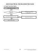
Страница 45: ... FUNCTION CHECK Check tuner module voltage Pin4 3 3 V NO Check tuner module TU500 operation YES YES Check IC501 Pin P8 P10 P11 T15 Check tuner module data NO YES Refer to function check 3 26 AUDIO ELECTRICAL TROUBLESHOOTIHG GUIDE ...

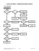
Страница 46: ...ck the signal 16 0344 MHz at IC407 Pin51 NO YES Check IC501 input output and control line NO YES YES Check loading motor NO IM driving Focus and tracking is ok NO Focus tracking sled signal is ok NO Check IC408 Motor drive IC NO Is the MD CN404 Pin22 about 190 mV YES Check Vcc of IC407 Check Cristal X400 NO Replace Cristal X400 Replace IC501 Check IC408 YES 1 CD FUNCTION Check IM pick up NO 3 27 C...

Страница 47: ...YES Plug in usb device Check CN302 NO NO YES Display READ YES Display NO FILE YES Check USB jack JK301 JK302 NO Replace IC501 NO Check IC501 Pin U7 U8 A7 A8 Check usb audio file in usb device MP3 WMA file is playable YES 2 DOUBLE USB FUNCTION 3 28 CDP ELECTRICAL TROUBLESHOOTIHG GUIDE ...

Страница 48: ...1 SDRAM 1 2 3 4 CLK DATA ADDRESS CS 2 SERVO 5 CD 16 M 3 29 WAVEFORMS OF MAJOR CHECK POINT IC502 PIN38 IC502 PIN53 IC502 PIN35 IC503 PIN1 IC501 PIN M1 ...

Страница 49: ...3 AUDIO PATH 6 7 8 CD_BCK CD_LRCK CD_DATA 3 30 IC501 PIN N4 IC501 PIN N1 IC501 PIN N2 9 10 12 11 DAC_MCLK DAC_BCK DAC_LRCK DAC_DATA IC501 PIN D2 IC501 PIN E1 IC501 PIN D1 IC501 PIN E2 ...

Страница 50: ...4 USB 13 USB_5 V D D 14 3 31 IC501 PIN A8 IC501 PIN A7 ...

Страница 51: ...3 32 ...

Страница 52: ...P SPK TERMINAL TUNER MODULE 1 CD MD MAIN CD 19P USB 2EA FRONT SMPS 15P AUX JACK 1 Total CNT 6 ea 1 FFC Cable MAIN FRONT 1 EA MAIN MD 2 EA MAIN BT module 1 EA 2 Harness Single SMPS MAIN 1 EA MAIN USB 1 EA Power cord 8P Harness FFC BT ...

Страница 53: ...K DAC_LRCK DAC_MCLK DRM_SEL DRM_CKE DRM_RAS DRM_CLK DRM_CAS DRM_WEN D0 D15 A0 A11 A13 A16 SF_DI DO SF_CS CLK SPI USB1_D IC511 IPOD 2 0C CP_RESET SCL SDA IC502 SDRAM IC503 FLASH W25Q16FVSSIG 8 MB 2 MB BT 4 0 New RX TX RTS CTS RST SDA SCL USB2_D PTB_SENSE SF_DI DO SF_CS CLK SPI IC504 FLASH W25Q80DVSSIG 1 MB Interrupt controller CDROM x8 speed Decoder NAND Controller within BCH codec 14bits ECC GDMA ...

Страница 54: ...ock X cap Line Filter Snubber Block Main SMPS IC Block T R A N S Snubber Block Photo coupler Photo coupler Photo coupler FL FL Vkk On Off 12 V LDO 12 V 5 6 VA P CTL On Off AMP SMPS IC With FET Block F U S E Y Cap Y Cap T R A N S CN901 Feedback Feedback ...

Страница 55: ...P Block PWM TAS5548 TAS5624LA FR FL Woofer Tuner Aux in ADC CS5346 SLAVE AUX MLC3730 176 PIN DAC_DATA DAC_LRCK DAC_BCK TUNER DAC_MCLK 12 288 MHz DAC_LRCK DAC_BCK TAS5624LA 230Wx2 240Wx1 RF LC78615E CD_BCK CD_LRCK CD_DATA ADC_DATA 32 768 KHz PORTABLE PORTABLE ...

Страница 56: ... 3 VA VFD 5 mA 3 mA 150 mA 25 mA 70 mA 5 V 370 mA 2 mA 2 668 A 100 mA 450 mA Pick up 80 mA 15mA 10 mA 20 mA 20 mA 160 mA ADC IC201 CS5346 20 mA 10 mA VKK FL 550 mA 1 A 601 mA Bluetooth Option 38 mA 310 mA Diode delete Diode delete CP Chip Option 7 mA 3 3 V IC701 AMP IC202 LDO LM37102D IC507 LDO TJ4220 IC506 RESET AZ7027 IC505 PWR SENS AZ7027 2 mA 2 mA 10 mA DVCC3 3 V USB HUB USB HUB To 3965 or 371...

Страница 57: ... SHADED ON THE SCHEMATIC FOR EASY IDENTIFICATION THIS CIRCUIT DIAGRAM MAY OCCASIONALLY DIFFER FROM THE ACTUAL CIRCUIT USED THIS WAY IMPLEMENTATION OF THE LATEST SAFETY AND PERFORMANCE IMPROVEMENT CHANGES INTO THE SET IS NOT DELAYED UNTIL THE NEW SERVICE LITERATURE IS PRINTED NOTE 1 Shaded parts are critical for safety Replace only with specified part number 2 Voltages are DC measured with a digita...

Страница 58: ...3 45 3 46 2 MAIN DSP CIRCUIT DIAGRAM 4 6 7 8 5 10 11 12 9 14 13 1 2 3 WAVEFORM NUMBER A 1 2 3 4 5 6 7 8 9 10 11 12 B C D E F G H I J K L M N O P Q R S T DSP EAX66325701 SD 01 _Rev6_1 1 2014 12 30 ...

Страница 59: ...3 47 3 48 3 MAIN SERVO CIRCUIT DIAGRAM A 1 2 3 4 5 6 7 8 9 10 11 12 B C D E F G H I J K L M N O P Q R S T SERVO EAX66325701 SD 02 _Rev6_1 1 2014 12 30 ...

Страница 60: ...3 49 3 50 4 MAIN ADC PWM CIRCUIT DIAGRAM A 1 2 3 4 5 6 7 8 9 10 11 12 B C D E F G H I J K L M N O P Q R S T ADC PWM EAX66325701 SD 03 _Rev6_1 1 2014 12 30 ...

Страница 61: ...3 51 3 52 5 MAIN AMP CIRCUIT DIAGRAM A 1 2 3 4 5 6 7 8 9 10 11 12 B C D E F G H I J K L M N O P Q R S T AMP EAX66325701 SD 04 _Rev6_1 1 2014 12 30 ...

Страница 62: ...3 53 3 54 6 FRONT CIRCUIT DIAGRAM A 1 2 3 4 5 6 7 8 9 10 11 12 B C D E F G H I J K L M N O P Q R S T FRONT EAX65586201_Rev2_1 2 2015 01 29 ...

Страница 63: ...5 VDD33USB20 3 0 3 6 3 24 3 24 U4 VDD12CORE 1 08 1 32 1 18 1 18 P4 VDD33IO 3 0 3 6 3 24 3 24 J4 VDD12INT 1 08 1 32 1 18 1 18 D4 VDD33IO 3 0 3 6 3 24 3 24 IC502 SDRAM W9812G6JH 6 1 VDD 3 0 3 6 3 24 3 24 3 VDDQ 3 0 3 6 3 24 3 24 9 VDDQ 3 0 3 6 3 24 3 24 14 VDD 3 0 3 6 3 24 3 24 27 VDD 3 0 3 6 3 24 3 24 43 VDDQ 3 0 3 6 3 24 3 24 49 VDDQ 3 0 3 6 3 24 3 24 Location Pin No SPEC EE Mode V Margin Playback...

Страница 64: ...V 0 V 1 19 V 14 81 V C579 10 uF 16 V 3 24 V 0 V 3 24 V 12 76 V 3 24 V 0 V 3 24 V 12 76 V C618 100 uF 16 V 3 25 V 0 V 3 25 V 12 75 V 3 25 V 0 V 3 25 V 12 75 V C624 100 uF 16 V 12 12 V 0 V 12 12 V 3 88 V 12 12 V 0 V 12 12 V 3 88 V C643 100 uF 16 V 5 08 V 0 V 5 08 V 10 92 V 5 08 V 0 V 5 08 V 10 92 V C724 470 uF 50 V 37 5 V 0 V 36 V 12 5 V 36 V 0 V 37 5 V 12 5 V C727 470 uF 50 V 37 5 V 0 V 36 V 12 5 V...

Страница 65: ...3 59 3 60 PRINTED CIRCUIT BOARD DIAGRAMS 1 SMPS P C BOARD NOTE Warning Parts that are critical with respect to risk of fire or electrical shock TOP VIEW BOTTOM VIEW ...

Страница 66: ...3 61 3 62 2 MAIN P C BOARD TOP VIEW BOTTOM VIEW ...

Страница 67: ...3 63 3 64 3 FRONT P C BOARD TOP VIEW BOTTOM VIEW ...

Страница 68: ... 2 2 2 Magnet 2 2 3 Clamp 2 3 Tray Disc 3 4 Pick Up Assembly 4 5 Base Up Down 4 6 Belt Loading 5 7 Gear Pulley 5 8 Gear Loading 5 9 Guide 5 10 Deck PCB Assembly 5 11 Motor Assembly 5 12 FFC Cable 5 DECK MECHANISM EXPLODED VIEW DP17TM3 6 APPENDIX MECHANISM DP17TM3 CONTENTS ...

Страница 69: ...mp Assembly as Figure B 2 Bending the Cover Top in direction of arrow 2 as Figure B 3 Separate the Clamp Assembly from the Cover Top 2 1 Plate 1 Turn the Plate to a counterclockwise direction and then lift up the Plate 2 Remove the Plate 2 2 Magnet Remove the Magnet 2 3 Clamp Remove the Clamp 1 3 S1 L1 Cover Top Figure A 2 1 2 Figure B Clamp Assembly Clamp Assembly Plate Magnet Clamp ...

Страница 70: ...ote When reassembling place the Guide as Figure E Tray Disc MD Sub Assembly Figure D 3 1 1 2 2 Tray Disc Figure E Guide 3 Tray Disc 1 Insert and push a flat head screwdriver in the Emergency eject hole H1 at the right side so that the Tray Disc is ejected about 15 20 mm 2 Pull the Tray Disc until it is locked Tray Disc Bottom side view Tray Disc Figure C 2 1 H1 Emergency eject hole ...
Страница 71: ...eassembling insert the D portion of the Base Up Down in the Hole H2 of the Base Main as Figure G 3 3 2 1 L2 Base Up Down Figure G 2 Figure G 1 C B Guide Base Up Down Base Main Figure G B H2 A Figure G 3 D 4 Pick Up Assembly 1 Detach the Gasket Tape 2 Disconnect the wires BLK RED BRN ORN from the Deck PCB Assembly by desoldering 3 Remove the 4 screws S2 4 Disconnect the FFC Cable from the Pick Up A...

Страница 72: ...B Assembly 1 Disconnect the wires RED BK form the Deck PCB Assembly by desoldering 2 Remove the 1 screw S3 3 Separate the Deck PCB Assembly from the Base Main 11 Motor Assembly Unlock the Locking Tab L4 in direction of arrow and then separate the Motor Assembly from the Base Main 12 FFC Cable Remove the FFC Cable Gear Pulley Belt Loading Deck PCB Assembly Motor Assembly Base Main Gear Loading Guid...

Страница 73: ...6 DECK MECHANISM EXPLODED VIEW DP17TM3 1026 1439 A001 1002 1005 1001 1049 1437 1437 1024 1024 1024 A006 1016 1013 1015 1020 1024 1003 1439 1018 1019 1011 1012 1437 1004 A005 1045 1043 1030 ...

Отзывы: