- 11 -
8. Tool Option Area Option Change
8-1. Profile
: Must be changed the option value because being different with
some setting value depend on module, inch and market.
8-2. Required Test Equipment
1) Adjustment remocon.
8-3. Adjustment method
Before PCB check, have to change the Tool option and Area option.
Option values are below.
(If on changed the option, the input menu can differ the model spec.)
The input methods are same as other chassises.(Use adj Key
on the Adjust Remocon)
9. Color carrier Adjustment
(Inspection process)
9-1. Profile
: To have the margin about the deviation of colorcarrier to
satisfy the spec.
9-2. Required Test Equipment
1) Adjustment remocon.
2) Pal RF signal.
9-3. Connection
: TV set should connected with the pal RF signal(EU 5CH).
9-4. Adjustment method
(1) tuning the RF signal
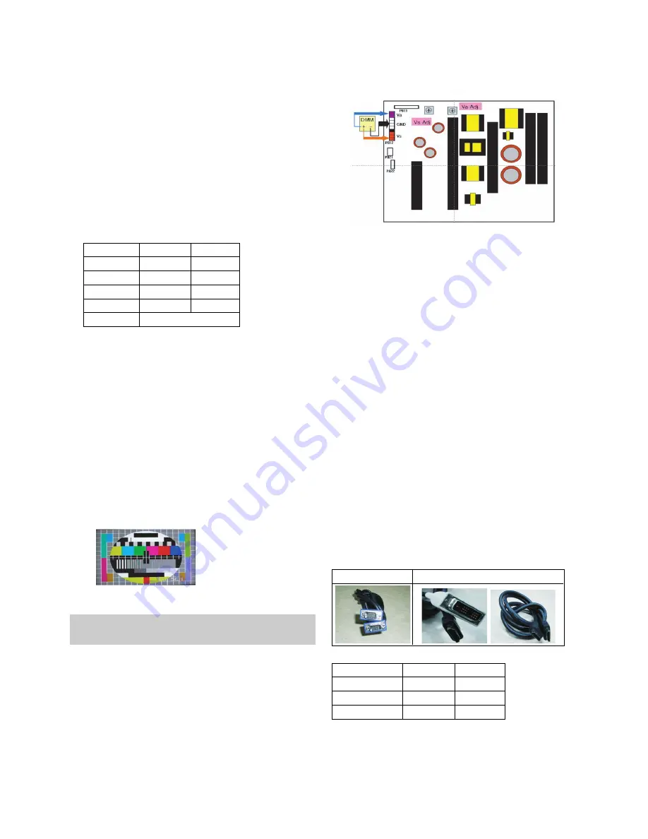
ZB, TB : PAL Philips Pattern (with Color Bar)
(2) push the “adj” key in the adjustment remocon.
10. POWER PCB Assy Voltage
Adjustments
(Va, Vs Voltage adjustments)
10-1. Profile
: To supply the Va, Vs voltage that the module want.
10-2. Required Test Equipment
(1) Stick for adjustment.
(2) DMM.
10-3. Connection structure
10-4. Connection Diagram for Measuring
: refer to (Fig. 1)
10-5. Adjustment Method
(1) Va Adjustment
1) After receiving 100% Full White Pattern, HEAT RUN.
2) C terminal of D. M..M. to Va pin of P812, connect
-terminal to GND pin of P812.
3) After turning VR901,voltage of D.M.M adjustment as
same as Va voltage which on label of panel right/top.
(deviation;
±0.5V)
(2) Vs Adjustment
1) C terminal of D. M..M. to Vs pin of P812, connect
-terminal to GND pin of P812.
2) After turning VR951, voltage of D.M.M adjustment as
same as Vs voltage which on label of panel right/top.
(deviation ;
±0.5V)
11. EDID
(The Extended Display Identification Data )
/DDC
(Display Data Channel)
download
11-1. Profile
: To be possible for plug and play.
11-2. EDID Data
* Caution
- Use the proper signal cable for EDID Download.
- Never connect HDMI & D-SUB Cable at the same time.
- Use the proper cables below for EDID Writing.
* EDID Data
Tool Option
Inch
ZB
TB
42(VGA)
02244
04292
42(XGA)
02252
04300
50
02260
04308
Area Option
Depend on PR
Item
Manufacturer ID
Version
Revision
Condition
GSM
Digital : 1
Digital : 3
Hex Data
1E6D
01
03
For RGB EDID
For HDMI EDID
(Fig. 1) Connection Diagram of power adjustment for measuring.
Each PCB assembly must be checked by check JIG set.
(Because power PCB Assembly damages to PDP Module,
especially be careful)
Содержание 42PC5R*
Страница 34: ......
Страница 35: ......
Страница 36: ......
Страница 37: ...MAIN TOP MAIN BOTTOM SIDE A V TOP SIDE A V BOTTOM IR LED CONTROL TOP CONTROL BOTTOM PRINTED CIRCUIT BOARD ...
Страница 38: ...Feb 2007 Printed in Korea P NO MFL34335201 ...


