background image

5. Adjustment Command

5.1. Adjustment Command (LENGTH=84)

5.2. EEPROM DATA READ

(1) Signal Table

(2) Command Set

Purpose : To read the appointment Address of E2PROM by

128(80h)-byte

5.3. E

2

PROM Data Write

(1) Signal Table

LEN

: 84h+Bytes

CMD

: 8Eh

ADH

: E

2

PROM  Slave Address(A0,A2,A4,A6,A8),

Not 00h(Reserved by BufferToEEPROM)

ADL

: E2PROM Sub Address(00~FF)

Data

: Write data

(2) Command Set

<Purpose>

1) EDID write : 16-byte by 16-byte, 8 order (128-byte) write

(TO “00 – 7F” of “EEPROM Page A4”)

2)FOS Default write : 16-mode data (HFh, HFl, VF, STD,

HP, VP, Clk, ClkPh, PhFine) write

3) Random Data write : write the appointment Address of

E2PROM

5.4. VRAM Read

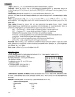
1) Send CMD(70h) to read Video RAM value from MICOM

And save its value to 128-Bytes Buffer(Common Buffer for
the use of EDID).

2) Delay 500ms(Time to wait and read vZideo RAM from

MICOM)

3) Be transmitted the contents of MICOM’s 128-bytes Buffer to

PC.(128th Data is the CheckSum of 127-bytes data : That’s
OK if the value of adding 128-bytes Data is Zero)

- 11 -

VAL

00

00

data

00

00 – 100

00 – 100

00 – 100

00 – 100

00 – FF

00 – FF

00 – FF

00 – 7F

00 – 7F

00 – 7F

00 – 3F

00 - 64

02

0, 1, 2, 3

00

00

Description

EEPROM all clear

EEPROM Read

EEPROM Write by

some values

Color Save

They have different

range each mode,

FOS Adjustment

Drive adjustment

Offset adjustment

Bright adjustment

Luminance adjustment

Auto COLOR

Adjustment

0: COOL

1: NORMAL

2: WARM

3: USER

00: Factory mode Off

FF:Factory mode On

0 : TV

1 : AV1

2 : AV2

3 : Component

4 : RGB

5 : DVI

No.

1

2

3

4

5

6

7

8

9

10

11

12

13

14

15

16

17

18

19

20

Adjustment Contents

EEPROM ALL INIT.

EEPROM Read

EEPROM Write

COLOR SAVE

(R/G/B cutoff, Drive,

Contrast, Bright)

H POSITION

V POSITION

CLOCK

PHASE

R DRIVE

G DRIVE

B DRIVE

R CUTOFF

G CUTOFF

B CUTOFF

BRIGHT

CONTRAST

AUTO_COLOR_

ADJUST

CHANGE_COLOR_

TEMP

FACTORY_

DEFAULT

AUTO_

INPUTCHANGE

CMD(hex)

E4

E7

E8

EB

20

30

90

92

16

18

1A

80

82

84

10

12

F1

F2

F3

F4

ADR

00

00

00

00

00

00

00

00

00

00

00

00

00

00

00

00

00

00

00

00

ST OP

A

A

A

A

A

50

6E

03

CMD

A DH

84+ n

ST ART

A DL

A

CS

A

A

Data_1

A

. . .

Data_n

A

No.

1

2

Adjustment contents

EEPROM WRITE

CMD(hex)

E8

LEN

94

84+n

Details

16-Byte Write

n-byte Write

ADL(hex)

0

80

0

80

0

80

0

80

Details

0-Page   0~7F  Read

0-Page  80~FF  Read

1-Page   0~7F  Read

1-Page  80~FF  Read

2-Page   0~7F  Read

2-Page  80~FF  Read

3-Page   0~7F  Read

3-Page  80~FF  Read

Adjustment Contents

EEPROM READ

CMD(hex)

E7

ADR(hex)

A0

A2

A4

A6

ST OP

A  D1 

6F 

ST OP 

ST ART 

A

Dn

A  50 

6E 

03 

CMD 

A DH 

84

ST ART 

A DL 

CS 

128 Bytes

Delay 100ms

A

CS 

A  Data1 

6F

ST ART

. . .  

Data12

ST OP

NA


ST OP

A  50 

6E 

03 

70 

00 

84 

ST ART 

00 

CS 

Содержание 17LS5R Series

Страница 1: ...LCD TV SERVICE MANUAL CAUTION BEFORE SERVICING THE CHASSIS READ THE SAFETY PRECAUTIONS IN THIS MANUAL CHASSIS LP68A MODEL 17LS5R 17LS5R ZA website http biz LGservice com ...

Страница 2: ... 2 CONTENTS CONTENTS 2 PRODUCT SAFETY 3 SPECIFICATION 6 ADJUSTMENT INSTRUCTION 9 TROUBLE SHOOTING 13 BLOCK DIAGRAM 17 EXPLODED VIEW 20 REPLACEMENT PARTS LIST 22 SVC SHEET ...

Страница 3: ...Current Cold Check Antenna Cold Check With the instrument AC plug removed from AC source connect an electrical jumper across the two AC plug prongs Place the AC switch in the on position connect one lead of ohm meter to the AC plug prongs tied together and touch other ohm meter lead in turn to each exposed metallic parts such as antenna terminals phone jacks etc If the exposed metallic part has a ...

Страница 4: ...y obtain and wear a commercially available discharging wrist strap device which should be removed to prevent potential shock reasons prior to applying power to the unit under test 2 After removing an electrical assembly equipped with ES devices place the assembly on a conductive surface such as aluminum foil to prevent electrostatic charge buildup or exposure of the assembly 3 Use only a grounded ...

Страница 5: ...not shiny reheat them and if necessary apply additional solder Fuse and Conventional Resistor Removal Replacement 1 Clip each fuse or resistor lead at top of the circuit board hollow stake 2 Securely crimp the leads of replacement component around notch at stake top 3 Solder the connections CAUTION Maintain original spacing between the replaced component and adjacent components and the circuit boa...

Страница 6: ...VDS Color Depth 6BIT WITH FRC 16 2M colors Size mm 385 5 W x 396 5 H x 15 8 D Max Surface Treatment Hard Coating 3H Anti Glare HAZE 3 Operating Mode Normally Black Back light Unit 4 CCFL 6 lamps R T Typ 5ms Typ 9ms Max No 1 Product Dimension Width W Length D Height H Before Packing 463 3 166 3 353 5 After Packing 527 175 470 2 Product Weight Only SET 3 94 kg CPT With BOX 5 04 kg CPT 3 Container In...

Страница 7: ...4 MTBF Hours Min Lamp Life 50 000 Hours MIN 5 Operating Environment Temp 10 35 deg Humidity 20 80 6 Storage Environment Temp 10 60 deg Non condensing Humidity 5 90 Non condensing 4 Optical Characteristic No Item Specification Remark Min Tpy Max 1 Viewing Angle R L 89 89 CR 10 U D 89 89 2 Luminance Luminance cd m2 320 400 PSM Dynamic CSM Cool White luminance uniformity 75 80 White 100 IRE 3 Contras...

Страница 8: ...annel Fine Search Name Programme Edit To set Favourite Programme Off 7 PICTURE PSM Dynamic Standard Mild Game User Contrast 100 Brightness 50 Colour 60 Sharpness 50 Tint 0 CSM Cool Normal Warm User Red 0 Green 0 Blue 0 Reset To set 8 SOUND SSM Flat Music Movie Sports User AVL Off Balance 0 9 TIME Clock Off time Off On time Pr 1 Vol 30 Off Auto sleep Off 10 SPECIAL Language English 16 Language Coun...

Страница 9: ...oad download file XXXX bin by clicking Read 4 Click Auto tab and set as below and then click Run 5 After downloading check OK message APC After Manual Insert executing APC 3 2 ADC Process 1 PC input ADC 1 Auto RGB Gain Offset Adjustment a Convert to PC in Input source b Signal equipment displays Output Voltage 730 mVp p Impress Resolution XGA 1024x768 60Hz Pattern gray pattern that left right is b...

Страница 10: ...me and then automatically LED is changed the stand by status RED Color Must not AC power OFF at that time 4 6 Option data setting SVC OSD setting Tool Option 20LS5R ZA REMARK 8 9 6 Resolution 0 Module 0 TV 1 SCART 1 AV2 1 COMPONENT 0 PC RGB 0 DVI 0 HDMI 0 Area Option A B A 0 FACTORY MODE OFF 1 FACTORY MODE ON Caution FACTORY MODE ON only used in factory B 0 default Option setting 1 4 The other Are...

Страница 11: ...r Save They have different range each mode FOS Adjustment Drive adjustment Offset adjustment Bright adjustment Luminance adjustment Auto COLOR Adjustment 0 COOL 1 NORMAL 2 WARM 3 USER 00 Factory mode Off FF Factory mode On 0 TV 1 AV1 2 AV2 3 Component 4 RGB 5 DVI No 1 2 3 4 5 6 7 8 9 10 11 12 13 14 15 16 17 18 19 20 Adjustment Contents EEPROM ALL INIT EEPROM Read EEPROM Write COLOR SAVE R G B cuto...

Страница 12: ...ch RGB WHITE MATRIX C B PHILIPS Crosshatch Crosshatch PHILIPS Colorbar Crosshatch Circle DIGITAL Crosshatch DIGITAL Crosshatch Colorbar DIGITAL DIGITAL DIGITAL DIGITAL Crosshatch 16 9 Monoscope Monoscope SMPTE Colorbar White Raster White Raster Crosshatch Circle Colorbar Philips Color Bar 2 Monoscope Color Bar 2 Color Bar Philips SECAM DK PAL BG PAL BG PAL I SECAM BG PAL BG PAL BG PAL BG PAL I PAL...

Страница 13: ...r off Check short of main B D or Change Lips Change IC903 Change LED Assy Check 15V or 5V of Lips Check Output of IC903 Check LED Assy Check P901 P270 Connector Fail Fail Change Q904 Check Output of Q904 Fail Pass Fail Pass Pass Pass A Process ...

Страница 14: ...C910 Check inverter connector or inverter Check inputting source cable and jack Repeat A PROCESS Fail Change IC900 IC901 IC906 IC908 IC909 IC910 Fail Change IC100 Fail Change inverter connector or inverter Fail Change panel link cable or module Fail Check panel link cable or module Pass Pass Pass Pass Pass B Process ...

Страница 15: ...0 L801 Check the signal of R104 R106 R108 R131 L822 L800 L801 Repeat A Process Check the output of TU500 Check the input output of IC100 Check inputting source cable and jack Fail Fail Fail Fail Re solder or change the defect part Check X101 Check 5V of TU500 Re solder or change the defect part Pass Pass Pass ...

Страница 16: ...input Check the input source Fail Pass Re solder or Change the defect part Check X301 Check the input output of IC100 Fail Pass Re solder or change the defect part Check the input output of IC400 Fail Pass Change the speaker Check the speaker Fail Pass ...

Страница 17: ...S Video Jack Stereo In Option H P Output LED IR Control Power Video Audio Data Address Data CLK DQM W EZ CASZ RASZ EEPROM 24C02 M12L16161A 5TG SDRAM CVBS Tuner CVBS Tuner SCL SDA SCL SDA SCL SDA SIF_OUT CVBS OUT MST96585 Scaler Video Decoder SCART Jack D Sub Option RS 232C Option Rx Tx CS4352 DAC 3 3V 12V Regulator Regulator Regulator Regulator Regulator 5V 1 8V LED IR Board Control MX232A RS 232C...

Страница 18: ...lock Selects input Video signals like CVBS Y C SCART RGB and output LVDS TTL signal through Scaler On decoding We can control signal like Contrast Brightness Sharpness Color tint signals including Adaptive Comb Filter 2 Audio Decoder This block analyzes audio input signal through A V Jack and PC audio and Tuner SIF The analyzed signals transmitted to audio amplifier On decoding We can control sign...

Страница 19: ... 19 MEMO ...

Страница 20: ... 20 300 200 580 520 591 590 120 521 800 400 530 531 431 433 432 100 521 EXPLODED VIEW ...

Страница 21: ......

Страница 22: ......

Страница 23: ...Feb 2007 Printed in Korea P NO MFL37159905 ...

Отзывы: