

Interfacing ispClock5600A
Lattice Semiconductor
with Reference Clock Oscillators
3
Reference and Feedback MUXes
The ispClock5620A has an input MUX for both the clock reference and the feedback inputs to the phase detect cir-
cuitry. If the select line for either MUX is asynchronously changed then it may result in a timing violation similar to
the waveforms shown in Figure 3. This also can result in an output phase relationship that would require the activa-
tion of the RESET pin to correct.
M and N Divider Bypass
Bypassing the M and N dividers will allow the ispClock device to accept clock pulses that are much shorter than the
t
CLOCKHI
or t
CLOCKLOW
specifications without resulting in unpredictable input to output phase relationships. The M
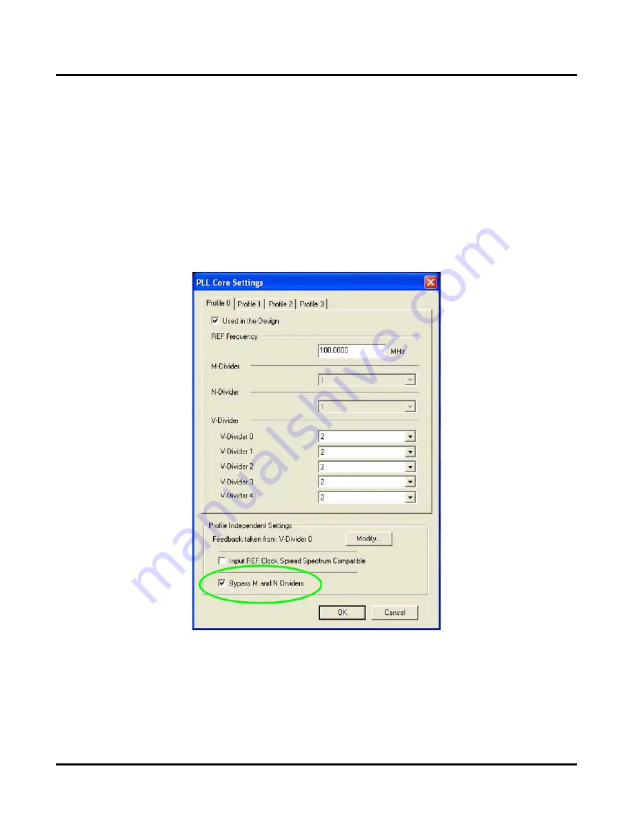
and N dividers can be placed in bypass mode by checking the box in the PLL Core Settings dialog box of PAC-
Designer, which is shown in Figure 4. Placing M and N into bypass mode results in a divider value of unity for both
M and N resulting in reduced frequency synthesis options.
Figure 4. Bypassing M and N Dividers in PAC-Designer
Summary
Activate the RESET pin after the reference clock is stable to prevent out of phase issues with the ispClock. When
Possible, M and N dividers can be bypassed to prevent out of phase issues.
Related Literature
• ispClock5600A Family Data Sheet


