Lattice Semiconductor ispClock5620A Скачать руководство пользователя страница 2


Interfacing ispClock5600A

Lattice Semiconductor

with Reference Clock Oscillators


2


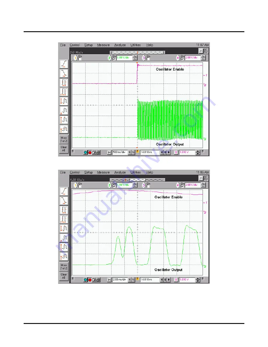
Figure 2. CMOS Oscillator Enabled

Figure 3. Initial Transitions of Enabled Oscillator


In this case where the reference oscillator is gated on, either by the output enable pin of the oscillator or by other
means of asynchronous enable, the RESET pin should be activated after the reference has been enabled and the
clock input to the ispClock is stable. 

Содержание ispClock5620A

Страница 1: ...k 5600A device This application note examines two common conditions when the reference oscillator clock could violate the tCLOCKHI or tCLOCKLOW specifications and warrant the activation of the RESET pin Powering Up Reference Oscillator After ispClock5600A Figure 1 details the start up behavior of a typical oscillator module Note that for the first 50ms the output is active the amplitude and offset...

Страница 2: ...d Figure 3 Initial Transitions of Enabled Oscillator In this case where the reference oscillator is gated on either by the output enable pin of the oscillator or by other means of asynchronous enable the RESET pin should be activated after the reference has been enabled and the clock input to the ispClock is stable ...

Страница 3: ...e ispClock device to accept clock pulses that are much shorter than the tCLOCKHI or tCLOCKLOW specifications without resulting in unpredictable input to output phase relationships The M and N dividers can be placed in bypass mode by checking the box in the PLL Core Settings dialog box of PAC Designer which is shown in Figure 4 Placing M and N into bypass mode results in a divider value of unity fo...

Страница 4: ...ce Clock Oscillators 4 Technical Support Assistance Hotline 1 800 LATTICE North America 1 503 268 8001 Outside North America e mail isppacs latticesemi com Internet www latticesemi com Revision History Date Version Change Summary August 2008 01 0 Initial release ...

Отзывы: