


www..lairdconnect.com/wireless
15
© Copyright 2020 Laird Connectivity. All Rights Reserved
Americas
: +1-800-492-2320
Europe
: +44-1628-858-940
Hong Kong
: +852 2923 0610
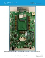
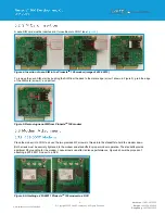
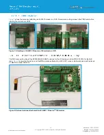
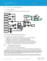
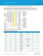
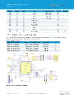
Figure 17 shows the DVK schematic of the M2 Connector (CON1), the IO headers (P1, P2, and P3), and the DIP switches
(S1, S2, S3, S4, and S5).
shows the interconnections between CON1, P1, and S1.
shows the
interconnections between CON1, P2, S2, and S5.
shows the interconnections between CON1, P3, S3, and S4.
Figure 17: M2, P1, P2, P3, S1, S2, S3, S4, and S5 schematic
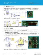
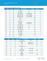
Table 1: P1 and S1 signal mapping to M2 pins
Header
Position
M2.#
Net
DVK Function
Switch
Position
P1
1
75
GND
P1
2
73
nBT_REST
SW5
S1
10
P1
3
71
nLTE_RESET
S1
9
P1
4
69
GND
P1
5
67
1V8_SIM
S1
8
P1
6
65
BAT_RTC
CR2032 Battery
S1
7
P1
7
63
GND
P1
8
61
P0.03_AIN1
SW2
S1
6
P1
9
59
P0.02_AIN0
SW4
S1
5
P1
10
57
GND
P1
11
55
P0.28_AIN4
VIN_ADC_EN
S1
4
P1
12
53
P0.29_AIN5
VIN_ADC
S1
3
P1
13
51
GND
P1
14
49
SIM_CLK
S1
2
P1
15
47
SIM_IO
S1
1
P1
16
45
GND
Содержание 453-00010-K1
Страница 1: ...Version 1 0 ...


