background image

2 - 1

Safety and Reliability

2. Safety and Reliability

2.1. Target group

This instruction manual contains all information necessary for
the use of the described product (control device, software, etc.)
according to instructions. It is written for the personnel of the
construction, project planning, service and commissioning
departments
. For proper understanding and error-free applica-
tion of technical descriptions, instructions for use and particu-
larly of notes of danger and warning, extensive knowledge of
automation technology
 is compulsory.

2.2. Reliability

Reliability of Kuhnke controllers is brought to the highest  pos-
sible standards by extensive and cost-effective means in their
design and manufacture.

These include:

selecting high-quality components,
quality arrangements with our sub-suppliers,
measures for the prevention of static charge during the hand-
ling of MOS circuits,
Worst-Case dimensioning of all circuits,
inspections during various stages of fabrication,
computer aided tests of all assembly groups and their
coefficiency in the circuit,
statistic assessment of the quality of fabrication and of all re-
turned goods for immediate taking of corrective action.

Despite these measures, the occurrence of errors in electronic
control units - even if most highly improbable - must be taken
into consideration.

Содержание KUAX 680C

Страница 1: ...Kuhnke Electronics Instruction Manual E 399 GB 16 January 1996 67 977 Compact Control KUAX 680C...

Страница 2: ...s only given to describe the product and must not be regarded as guaranteed properties in the legal sense Any claims for damages against us on whatever legal grounds are excluded except in instances o...

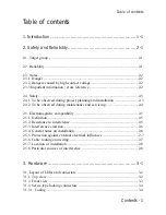
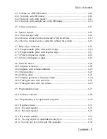
Страница 3: ...2 To be observed during maintenance and servicing 2 4 2 5 Electromagnetic compatibility 2 5 2 5 1 Definition 2 5 2 5 2 Resistance to interference 2 5 2 5 3 Interference emission 2 6 2 5 4 General note...

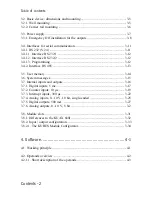
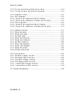
Страница 4: ...ce RS 485 3 13 3 5 User memory 3 14 3 6 System messages 3 15 3 7 Internal inputs and outputs 3 16 3 7 1 Digital inputs 5 ms 3 17 3 7 2 Counter inputs 10 s 3 19 3 7 3 Interrupt inputs 300 s 3 22 3 7 4...

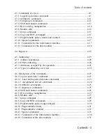
Страница 5: ...nics 4 20 4 5 2 Offset addressing 4 20 4 5 3 Addresses occupied by the operands 4 21 4 5 4 Types of addressing overview 4 22 4 6 Description of the commands 4 23 4 6 1 Logical operations commands 4 23...

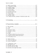
Страница 6: ...s 4 45 5 Networking 5 1 6 Programming examples 6 1 6 1 Basic functions 6 1 6 1 1 AND 6 1 6 1 2 OR 6 1 6 1 3 Negation at input 6 2 6 1 4 Negation at output 6 2 6 1 5 NAND 6 3 6 1 6 NOR 6 3 6 1 7 XO EXC...

Страница 7: ...negative edge 6 17 6 7 3 Pulse with positive signal 6 18 6 7 4 Pulse with negative signal 6 19 6 8 Software timers 6 20 6 8 1 Impulse at startup 6 20 6 8 2 Impulse with constant duration 6 21 6 8 3 Ra...

Страница 8: ...6 6 15 Arithmetic functions 6 37 6 15 1 Binary 8bit adder 6 37 6 15 2 Binary 16bit adder 6 37 6 15 3 8bit BCD adder 6 38 6 15 4 Binary 8bit subtractor 6 39 6 15 5 Binary 16bit subtractor 6 39 6 15 6 8...

Страница 9: ...1 C 1 Trademarks C 1 D Reactions to failures D 1 D 1 Short circuit on an output failure 1 D 3 D 2 Undervoltage supply failure 2 D 4 D 3 Watchdog program run time exceeded failure 3 D 6 D 4 Checksum in...

Страница 10: ...Contents 8 Table of contents...

Страница 11: ...485 with separate connection 16 digital inputs 2 counter inputs for fast event counting 2 interrupt inputs 4 analog inputs 16 digital outputs 2 analog outputs Should you need more you can extend the...

Страница 12: ...1 2 Introduction...

Страница 13: ...liability of Kuhnke controllers is brought to the highest pos sible standards by extensive and cost effective means in their design and manufacture These include selecting high quality components qual...

Страница 14: ...escribed precautions are not taken 2 3 2 Dangers caused by high contact voltage This symbol warns you of dangers of death or grievous bodily harm which may be caused by high contact voltage if the de...

Страница 15: ...be realized in accordance with EN 60204 IEC 204 VDE 0113 They must be effective at any time Safety and precautions regulations for qualified applications have to be observed Please pay particular att...

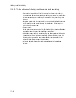
Страница 16: ...y the trained Kuhnke person nel usually in the main factory in Malente Warranty ex pires in any other case Spare parts Only use parts approved of by Kuhnke Only genuine Kuhnke modules must be used in...

Страница 17: ...ends on the exact location It is determined in the relevant product standards The international standard regulating construction and degree of noise resistance of programmable logic controllers is IEC...

Страница 18: ...s are fitting the controller into a grounded metal cabinet and equipping the supply cables with filters 2 5 4 General notes on installation As component parts of machines facilities and systems elec t...

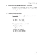
Страница 19: ...ference Ensure practical wiring and laying of cables 2 5 6 Cable routing and wiring Separate laying of power supply circuits never together with control loops DC voltage 60 V 400 V AC voltage 25 V 400...

Страница 20: ...vehicles Electromagnetic interference Consider electromagnetic interference from various sources near the location of installation motors switching devices switching thyristors radio controlled devic...

Страница 21: ...s 2 counter inputs 24 V DC counting frequency 10 kHz 2 interrupt inputs 24 V DC 0 3 ms 4 analog inputs 0 10 V 10 bit single ended 16 digital outputs 24 V DC 0 5 A 2 analog outputs 0 10 V 8 bit Module...

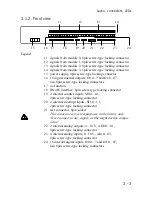
Страница 22: ...ector 8 normal program load monitor switch pos L normal program pos R load monitor Don t change the switch position in run mode Otherwise the program run is interrupted 9 plastic knobs to lock the mod...

Страница 23: ...locking connector 19 2 internal counter inputs SI0 0 0 1 2pin screw type locking connector 20 2 internal interrupt inputs SI1 0 1 1 2pin screw type locking connector 21 test connector 8pin socket This...

Страница 24: ...screwdriver with a wide blade as a lever Never pull the leads to unplug locking connectors You might otherwise accidentally pull them out of the terminals or rip them off 3 1 3 1 Coding The MINI COMBI...

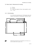
Страница 25: ...il 7 5 mm 3 2 1 Wall mounting Use 5 M4 screws to attach the device The illustration shows the positions of the drill holes in the base plate of the KUAX 680C Dimensions and positions of the drill hole...

Страница 26: ...this purpose use 3 for devices with 8 slots These must be ordered separately see appendix B 1 Accesso ries Lengthways the base plate provides 6 T slots two of which are used as a casing for the nuts f...

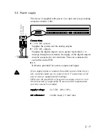
Страница 27: ...e supply of the digital outputs must be connected to two terminals These are connected to each other on the PCB 0 V Reference potential for system outputs and inputs If you supply inputs or outputs fr...

Страница 28: ...puts while the output power supply is switched off e g by emergency off installation This is valid in cases where the system is still supplied with power Wrong Outputs set by the program can be suppli...

Страница 29: ...ther switching elements in this case the test switch to the emergency off installation if the switches are connected in parallel to the outputs Emergency Off installation power supply 24 V DC emergenc...

Страница 30: ...ply voltages For reasons of operational safety the 0V potential of the KUAX 680C has a capacitive connection to the frame ground High fre quency interferences can bleed off via this connection Shieldi...

Страница 31: ...ion of these interfaces i e the configura tion without any influence by KUBES modules is as follows protocol KUBES protocol tranfer rate 9600 baud data bits 8 parity check o odd stop bits 1 type of co...

Страница 32: ...4 1 3 Programming Programs for the KUAX 680C are written using KUBES the Kuhnke user software as from version 4 12 KUBES runs on PCs under the Windows user interface version 3 1 or better As long as t...

Страница 33: ...ermin K K C remove coding element Connectors from left to right Shield cabel shield incoming Data data line incoming Data data line incoming Shield cable shield outgoing Data data line outgoing Data d...

Страница 34: ...odule will thus become invalid dead module Like this some memory space is lost with every edit ing process The free memory is indicated in the KUBES Main Status bar Transmitting the entire changed pro...

Страница 35: ...he de vice is not supplied with power data security can therefore only be guaranteed for a limited amount of time see appendix A Technical specifications We therefore recommend not to use the RAM as p...

Страница 36: ...g signals analog signals analog signals analog signals analog signals such as temperature values liquid level values speeds etc In the chapter below you will find descriptions of the inputs and output...

Страница 37: ...switching thresholds Defined signals and switching thresholds logical 0 5 V logical 1 15 V hysteresis 1 4 V Signal delay Signal delay Signal delay Signal delay Signal delay Voltage surges noise impul...

Страница 38: ...0 01 E00 02 E00 03 E00 04 E00 05 E00 06 E00 07 E01 00 E01 01 E01 02 E01 03 E01 04 E01 05 E01 06 E01 07 read E I Technical specifications number of inupts 16 type to IEC 1131 1 potential separation no...

Страница 39: ...thresholds logical 0 5 V logical 1 15 V hysteresis 1 4 V Signal delay Signal delay Signal delay Signal delay Signal delay Voltage surges noise impulses are filtered out to avoid them being accepted as...

Страница 40: ...00 SE00 01 read SE SI Technical specifications number of inputs 2 function counter inputs type to IEC 1131 1 potential separation no line interfacing 2pin screw type locking connector 3 81 matrix indi...

Страница 41: ...unication be tween user program and counters SLI00 00 00 15 counter 1 SLI01 00 01 15 counter 2 The operands of the transfer buffer memory have the following significance SLI0x 00 actual lowbyte value...

Страница 42: ...ignals and switching thresholds logical 0 5 V logical 1 15 V hysteresis 1 4 V Signal delay Signal delay Signal delay Signal delay Signal delay Voltage surges noise impulses are filtered out to avoid t...

Страница 43: ...I Technical specifications number of inputs 2 function counter inputs type to IEC 1131 1 potential separation no line interfacing 2pin screw type locking connector 3 81 matrix indicators LEDs location...

Страница 44: ...r memories is to determine whether an input is to trigger an interrupt and which input if so After the occurrence of an interrupt the transfer buffer memory will contain the interrupt source The opera...

Страница 45: ...e il lustration given in chapter 3 1 2 Front view pos 23 to find the exact location of the connectors AE00 00 Gnd AE00 01 Gnd AE00 02 Gnd AE00 03 Gnd K K C remove coding element read AE AI It is oblig...

Страница 46: ...Settings Settings Settings Analog conversion must be enabled by the user program if and when required Enabling will be automatic if the device is configured with an additional analog input module You...

Страница 47: ...04 A00 05 A00 06 A00 07 A01 00 A01 01 A01 02 A01 03 A01 04 A01 05 A01 06 A01 07 read A O Reverse polarity protection Reverse polarity protection Reverse polarity protection Reverse polarity protection...

Страница 48: ...s and notifies the CPU of the short circuit the CPU outputs a short circuit message reports the short circuit by a flashing rhythm 1 of the fail ure LED activates interrupt module 18 see also appendix...

Страница 49: ...connection Signal line connection Signal line connection The output signal lines are connected to the front of the device via a 4pin screw type locking connector Please refer to the il lustration give...

Страница 50: ...value is contained in bits 7 14 the sign bit bit 15 is 0 Bits 0 6 are not analysed Address bit 15 14 13 12 11 10 9 8 7 6 5 4 3 2 1 0 Status x value to be output x x x x x x x In the user program the v...

Страница 51: ...do not fit into the slots of the KUAX 680C They have no drilled hole at the bottom for locking the module into place see chapter 3 2 2 Top view pos 9 The four plug in connectors for the modules are l...

Страница 52: ...e same system resources i e the PWM outputs of the processor PWM analog output stepping motor module 1 AO00 00 680 444 01 und 02 2 AO00 01 680 444 02 Thus if you are working with a two channel steppin...

Страница 53: ...uts 1 Additional 2 x stepping motor PWM 1 Additional 2 x stepping motor PWM or 2 x analog input 2 Addi 4 x a 2 Enter the inputs and outputs that the device is equipped with into the KUBES Module Confi...

Страница 54: ...ts 4 to 7 are reserved for the internal configuration The entries for slots 4 and 5 cannot be changed The entries for slots 6 and 7 stand for the internal inputs and outputs Enter I O modules of the s...

Страница 55: ...s all programs for controlling the machine or plant The programs are written under the KUBES programming software Another feature is so called C tasks which can be included in the user program C tasks...

Страница 56: ...6 256 256 256 DB000 00 DB100 00 DB200 00 DB300 00 DB400 00 DB500 00 DB600 00 DB700 00 DB015 15 DB115 15 DB215 15 DB315 15 DB415 15 DB515 15 DB615 15 DB715 15 You can use these operands like normal byt...

Страница 57: ...ol bus Outputs output control signals to relays contactors magnets etc in order to switch them on or off Determined by the user program the CPU transmits the signals to the output modules via the cont...

Страница 58: ...analog values of temperatures liquid levels speeds etc The analog digital conversion is done by the pro cessor The digital value can be processed in the program Outputs output analog control signals...

Страница 59: ...d as they may lead to wrong results 4 3 1 Logical operations commands Logical operations commands are commands which serve the logical operation between operands including the assignment of results Th...

Страница 60: ...00 00 10 BM00 00 BM01 00 6 6 10 16 10 16 0 83 0 83 1 38 4 63 1 38 4 63 load negation 1bit address load negation 8bit address load neg 1bit address with constant offset load neg 1bit address with varia...

Страница 61: ...0 I00 00 10 I00 00 BM01 00 BM00 00 10 BM00 00 BM01 00 BM00 00 SLA01 00 8 8 12 18 12 18 18 1 13 1 13 1 63 4 83 1 63 4 83 4 83 AND negation 1bit address AND negation 8bit address AND neg 1bit address wi...

Страница 62: ...s yes yes yes yes ON I00 00 BM00 00 I00 00 10 I00 00 BM01 00 BM00 00 10 BM00 00 BM01 00 8 8 12 18 12 18 1 13 1 13 1 63 4 83 1 63 4 83 OR negation 1bit address OR negation 8bit address OR negation 1bit...

Страница 63: ...tant offset Excl OR 8bit slave addr with variable offset yes yes yes yes yes yes yes XON I00 00 BM00 00 I00 00 10 I00 00 BM01 00 BM00 00 10 BM00 00 BM01 00 8 8 12 18 12 18 1 13 1 13 1 63 4 83 1 63 4 8...

Страница 64: ...8bit address Assignment neg 1bit addr with const offset Assignment neg 1bit addr with var offset Assignment neg 8bit addr with const offset Assignment neg 8bit sl addr with var offset yes yes yes yes...

Страница 65: ...yes yes yes yes yes MUL BM00 00 100 8 10 4 4 13 Multiplication 8bit address Multiplication 8bit constant 0 0 yes yes MULD BM00 00 BM00 01 10000 8 12 8 3 63 6 38 3 38 Multiplication 16bit address even...

Страница 66: ...dress Compare if inequal 8bit constant yes yes yes yes CMPD BM00 00 BM00 01 10000 18 22 16 2 25 5 25 2 0 Compare if inequal 16bit address even Compare if inequal 16bit address odd Compare if inequal 1...

Страница 67: ...dd yes yes LSRDM BM00 00 BM00 01 10 14 1 75 7 25 Log shift right in 16bit address Log shift right in 16bit address odd yes yes ROL Accu 2 0 25 Roll left in accu 8bit yes yes ROR Accu 10 1 25 Roll righ...

Страница 68: ...LC 2 0 25 Clear Carry bit 0 yes Influence on C arry and Z ero bit yes no change defined flag alteration undefined flag alteration Com mand Operand example Byte Time s Function C Z JPP Program module 1...

Страница 69: ...ark 4 0 5 Jump if positive two s complement JP Jump mark 4 0 5 Jump if negative two s complement Times the higher value is valid if there is a jump the smaller value is valid if there is no jump Influ...

Страница 70: ...4 4 4 0 63 0 63 0 63 logical operation with time output LN AN ON PT00 00 6 8 8 0 88 1 13 1 13 logical operation with time output negated C00 00 100 V R 14 13 5 set progr counter with const cnt value...

Страница 71: ...ry and Z ero Bit yes no change defined flag alteration undefined flag alteration Operand Data type Value Byte Time s Function O00 00 BIT 1 1 0 1 1 16 1 Write logical value into 1bit address Write logi...

Страница 72: ...x 0 7 byte1 byte2 load data module number y y value 1 255 in byte2 intoDBx00 00 15 15 x value 0 7 in byte1 StoreDB x name store DBx00 00 15 15 x 0 7 in data module name byte1 name store DBx00 00 15 15...

Страница 73: ...t stands for a chargeable battery 1bit operands are used for internal byte operations Only bit 7 of the 8bit accu is analysed however For 16bit operands a 16bit accu is used which uses the above menti...

Страница 74: ...ute address and offset L BM00 00 BM00 01 means that the value in BM00 01 offset is added to the address of BM00 00 The resulting new address then responds to the load command The value of the offset s...

Страница 75: ...B900 0B9FF 09C00 09CFF BZ CPU 0BA00 0BAFF 09D00 09DFF T 0BB00 0BBFF 09E00 09EFF global variables 0BC00 0BC0F 09F00 09FFF ERR00 00 0BC10 0BC10 BM 0A000 0AFF0 global variables 0BC11 0BCFF SBM 0A100 0A1F...

Страница 76: ...constant 0 65535 LD 10000 decimal LD 3FEA hexadecimal LD 0010011100010000 binary LD 4 5V voltage 10 10V LD 5mA current 20 20mA To load the contents of an offset addressed operand with constant offset...

Страница 77: ...OD logical OR operation Logical OR operation bit by bit between the value of the operand and the contents of the accu The result of the operation is stored in the accu XO logical exclusive OR operati...

Страница 78: ...after the preceding operation it remains unchanged if there is log 0 in the accu R conditional reset Sets the value of the operand to log 0 if there is log 1 in the accu after the preceding operation...

Страница 79: ...he value of the operand to the contents of the accu The operation sets internal flags These lead to conditional jump instructions and are used for program branching CMP CMPD Compare if equal Like Comp...

Страница 80: ...dividing the contents by 2 The result of the operation is stored in the operand ROL ROLD Roll end around shift left in the accu by Carry Shifts the contents of the accu by one binary position The cont...

Страница 81: ...dule calls Cmnd Function JPP unconditional call of a program module JPCP conditional call of a program module Calls the module up if the accu contains a bit operand set to logical 1 bit 7 is read JPF...

Страница 82: ...p if the accu contains a bit operand set to logical 1 bit 7 is read JPCN conditional jump if no log 0 Carries out the jump if the accu contains a bit operand set to logical 0 bit 7 is read Conditional...

Страница 83: ...accu C8T1 copies the value of 8bit accus into eight 1 bit operands C16T1 copies the value of 16bit accus into sixteen 1 bit operands BINBCD3 Binary to BCD conversion into a 3 decade BCD value Before t...

Страница 84: ...pulse L I00 00 map input M00 00 on marker Command Function L I00 00 PP00 00 The programmable pulse output is set when the status of the input changes from 0 to 1 The programmable pulse output is rese...

Страница 85: ...the software timer at edge 0 1 Stop and RESET at log 0 Examples PT01 00 175 100ms R R Start raising delay of 17 5 s with remanent actual value PT01 00 BM04 06 100ms F R Start falling delay with varia...

Страница 86: ...ESET at log 0 Examples C00 00 175 F Start forward counter with preset value 175 C01 01 BM00 00 B R Load remanent backward counter with variable preset value is in BM00 00 and BM00 01 To scan an output...

Страница 87: ...rs and stops program execution Restart is only possible by switching the supply off and on again Use for example to react to very extensive times of undervoltage see appendix D Reactions to failures W...

Страница 88: ...le byte as binary value single byte as ASCII character BM00 00 BM00 00 BYTE BYTE 1 18 0 125 8 128 byte string with different values byte string with max 255 equal values WORD Assigns values to one or...

Страница 89: ...ata processing range DBx00 00 15 15 x 0 7 byte1 name loads the contents of data module name into data processing range DBx00 00 15 15 x value 0 7 in byte1 x byte2 loads the contents of data module num...

Страница 90: ...4 36 Description of the commands...

Страница 91: ...ules timer modules interrupt modules initialization modules data modules trigger modules KUBES modules The watchdog monitors the cycle time The processing of the individual modules is monitored by a w...

Страница 92: ...programming of the organization module should include program selection and calling of the modules responsible for overall tasks All commands are applicable without limitations commands of the initia...

Страница 93: ...variables operands constants These parameters are entered into a table and are used in the program part like normal operands under their own names Multiple use with different parameters in one program...

Страница 94: ...ble timers The timer modules created by the user are called up and processed by these time interrupts All commands are applicable without limitations module calls and commands of the initialization mo...

Страница 95: ...f the initialization modules excluded Call by modules that can trigger interrupts Call by modules that can trigger interrupts Call by modules that can trigger interrupts Call by modules that can trigg...

Страница 96: ...01 15 SLF00 00 01 15 5 6 module 3 SLG00 00 01 15 SLH00 00 01 15 7 8 internal counters SLI00 00 01 15 internal interrupt inputs SLJ00 00 01 15 10 internal analog inputs SLK00 00 01 15 error message vol...

Страница 97: ...le see chapter 4 6 13 Commands of the initialization modules Initialization modules should only be called when needed but not cyclically cycle time 4 7 7 Data module Name xxxxxxxx DAT Number 255 Lengt...

Страница 98: ...of the lowbyte in the accu is analysed 4 7 9 KUBES module Name set KNK Number 255 Parameters max 16 Function Module for special solutions Call from the organization and the program module Created by K...

Страница 99: ...4 45 Software 4 7 10 Module hierarchy example for different module calls...

Страница 100: ...ed up automatically Interrupt modules INT they are called up by function modules Timer modules TIM they are called up by time interrupts 2 Modules which are called up by a program command 3 Virtual mo...

Страница 101: ...r the built in serial RS 485 interface allows communi cation with less extended protocols Details concerning network communication were not available at the copy deadline of this edition of the instru...

Страница 102: ...5 2 Networking...

Страница 103: ...KUAX 680C inputs and outputs are counted octally channels 08 15 do not exist They can be arbi trarily replaced however 6 1 Basic functions 6 1 1 AND Circuit diagram Function diagram Instruction list...

Страница 104: ...6 2 Examples 6 1 3 Negation at input Circuit diagram Function diagram Instruction list LN I00 04 O00 02 6 1 4 Negation at output Circuit diagram Function diagram Instruction list L I00 05 N O00 03...

Страница 105: ...6 3 Examples 6 1 5 NAND Circuit diagram Function diagram Instruction list L I00 06 A I00 07 N O00 04 6 1 6 NOR Circuit diagram Function diagram Instruction list L I00 08 O I00 09 N O00 05...

Страница 106: ...O EXCLUSIVE OR non equivalence Circuit diagram Function diagram Instruction list L I00 10 XO I00 11 O00 06 6 1 8 XON EXCLUSIVE NOR equivalence Circuit diagram Function diagram Instruction list L I00 1...

Страница 107: ...6 5 Examples 6 1 9 Self locking circuit Circuit diagram Function diagram Instruction list L I00 14 O O00 08 AN I00 15 O00 08...

Страница 108: ...00 O00 09 6 2 2 With set dominance Circuit symbol Instruction list L I00 02 R M00 01 L I00 03 S M00 01 L M00 01 O00 10 If in controls that work without process mapping the set and reset inputs are act...

Страница 109: ...uits 6 3 1 OR AND circuit Circuit diagram Function diagram Instruction list L I00 04 ON I00 05 A I00 06 O00 11 6 3 2 Parallel circuit to output Circuit diagram Function diagram Instruction list LN I00...

Страница 110: ...6 8 Examples 6 3 3 Network with one output Circuit diagram Function diagram Instruction list L I00 15 ON I00 00 A I00 01 O O00 14 AN I00 02 O00 14...

Страница 111: ...work with outputs and markers Circuit diagram Instruction list Function diagram L I00 12 O M00 02 AN I00 13 AN I00 14 M00 02 L I00 15 O M00 03 AN M00 02 AN I00 14 M00 03 L M00 02 AN I00 00 O00 04 LN M...

Страница 112: ...Function diagram Instruction list L I00 01 Note In this example a part result A I00 02 has to be stored temporarily SM15 15 Definition S marker SM15 15 is basically L I00 03 always used as OR marker A...

Страница 113: ...struction list Note In this example too a L I00 05 result has to be stored O I00 06 temporarily in an S marker SM15 14 This marker is linked in L I00 07 an AND operation O I00 08 Definition S marker 1...

Страница 114: ...e of the OR marker Circuit diagram Function diagram Instruction list L I00 00 A I00 01 SM15 15 set OR marker L I00 02 A I00 03 O SM15 15 SM15 14 set AND marker L I00 04 A I00 05 SM15 15 set OR marker...

Страница 115: ...tion list after L I00 00 L I00 03 A I00 01 A I00 04 SM15 14 O I00 02 L I00 02 A I00 00 SM15 15 A I00 01 L I00 03 O00 12 A I00 04 O SM15 15 A SM15 14 O00 12 Circuit conversion leads to a different sequ...

Страница 116: ...6 14 Examples 6 6 Special circuits 6 6 1 Current surge relay Signal course Instruction list L I00 00 PP00 00 L PP00 00 XO O00 00 O00 00...

Страница 117: ...out forced halt Circuit diagram Instruction list 1 L I00 01 right key switch O O00 00 right contactor AN I00 02 left key switch AN O00 01 left contactor AN I00 00 stop key 2 O00 00 right contactor L I...

Страница 118: ...ses for status change recogni tion of logical signals edge evaluation They can be used for both the positive and the negative edge 6 7 1 Programmable pulse with positive edge Circuit diagram Switching...

Страница 119: ...r switching the controller on After switching the controller on or after a RESET the pulse has to be passed once at a value of 0 as the function cannot be guaranteed otherwise Recommendation Assign a...

Страница 120: ...eversals the signal status is evaluated in the following two examples This causes a different behavior when switching the control on 6 7 3 Pulse with positive signal Circuit diagram Switching symbol I...

Страница 121: ...6 19 Examples 6 7 4 Pulse with negative signal Circuit diagram Switching symbol Instruction list LN I00 03 SM15 14 AN M00 01 O00 03 L SM15 14 M00 01 Signal course T 1 cycle...

Страница 122: ...6 20 Examples 6 8 Software timers 6 8 1 Impulse at startup Circuit diagram Switching symbol Instruction list L I00 01 PT00 01 135 10ms P L PT00 01 O00 01 Signal course T Time preselection here 1 35s...

Страница 123: ...21 Examples 6 8 2 Impulse with constant duration Circuit diagram Switching symbol Instruction list L I00 02 O PT00 02 PT00 02 123 100ms P L PT00 02 O00 02 Signal course T Time preselection here 12 3s...

Страница 124: ...6 22 Examples 6 8 3 Raising delay Switching symbol Instruction list L I00 03 PT00 03 185 10ms R L PT00 03 O00 03 Signal course T Time preselection here 1 85s...

Страница 125: ...6 23 Examples 6 8 4 Falling delay Switching symbol Instruction list L I00 04 PT00 04 35 100ms F L PT00 04 O00 04 Signal course T Time preselection here 3 5s...

Страница 126: ...24 Examples 6 8 5 Impulse generator with pulse output Switching symbol Instruction list L I00 05 AN O00 05 PT00 05 55 10ms R L PT00 05 O00 05 Signal course T1 Time preselection here 0 55s T2 Cycle tim...

Страница 127: ...6 25 Examples 6 8 6 Flash generator with one timer Switching symbol Instruction list L I00 06 PT00 06 50 10ms C L PT00 06 O00 06 Signal course T Time preselection here 0 50s Flash frequency 1 Hz...

Страница 128: ...timers Switching symbol Instruction list L I00 00 AN PT00 02 PT00 01 5 100ms P L PT00 01 O00 00 LN PT00 01 PT00 02 10 100ms P Signal course T1 Time preselection for switch on here 500ms 0 5s T2 Time...

Страница 129: ...the next clock pulse causes a carry to 0 Example for an application Each part of the program is supposed to be passed only every 100 ms P1_STA L PC00 01 is 100 ms clock pulse memory CMP BM03 14 equal...

Страница 130: ...Forward counter to 12 L I00 00 start counter C00 00 12 F L I00 01 count transfer clock pulse C C00 00 L C00 00 scanning Count completed A00 12 LD C00 00 scan actual value D BM00 00 6 11 Programming o...

Страница 131: ...SM00 03 Step 3 R O00 00 Cylinder A S O00 02 Cylinder C L I00 01 Limit switch a0 A I00 06 Limit switch c1 A SM00 03 Step 3 AN SM00 04 Step 4 S SM00 04 Step 4 S O00 00 Cylinder A R O00 01 Cylinder B L...

Страница 132: ...6 30 Examples...

Страница 133: ...06 1bit shift reg Instruction list L I00 00 shift clock pulse PP00 00 pulse L PP00 00 pulse JPCN NORM to normal program if no L O00 05 step 5 O00 06 step 6 L O00 04 step 4 O00 05 step 5 L O00 03 step...

Страница 134: ...g Instruction list L I00 00 shift clock pulse PP00 00 pulse L PP00 00 pulse JPCN NORM to normal program if no L BM00 05 step 5 BM00 06 step 6 L BM00 04 step 4 BM00 05 step 5 L BM00 03 step 3 BM00 04 s...

Страница 135: ...the same way the con tents of byte operands can be copied directly into the 1bit range 6 13 1 To copy eight 1bit operands into one byte C1T8 I00 00 copy contents of I00 00 I00 07 into the accumulator...

Страница 136: ...bytes C1T16 I01 00 load contents of I01 00 I01 15 into the accumulator D BM00 02 copy contents of the accumulator into BM00 02 BM00 03 I01 00 I01 07 into BM00 02 I01 08 I01 15 into BM00 03 6 13 4 To...

Страница 137: ...V1 to V2 CMP BM00 01 whether greater or equal 1 O00 00 CA becomes 1 if V1 is greater or equal or otherwise 0 1 further commands are CMP CMP CMP 6 14 1 2 Result of the comparison evaluation with one j...

Страница 138: ...mpare V1 to V2 CMPD BM00 01 whether greater or equal 1 O00 00 CA is set if V1 is greater or equal 1 further commands are CMPD CMPD CMPD 6 14 2 2 Result of the comparison evaluation with one jump The r...

Страница 139: ...y 16bit adder BM00 01 Z1 BM00 03 Z2 Z3 BM00 05 binary 16bit adder Program LD BM00 00 Z1 1st summand ADDD BM00 02 Z2 2nd summand D BM00 04 Z3 sum In case of a carry the carry bit is set Z1 1st summand...

Страница 140: ...upper 4 bits LBM00 00 1st decade of this L BM00 01 Z2 2nd summand A 00001111 1st decade of this ADD LBM00 00 CMP 10 BCD correction necessary JP ADDIT jump if not L 6 load correction LBM00 01 value if...

Страница 141: ...rahend BM00 02 Z3 difference 6 15 5 Binary 16bit subtractor BM00 01 Z1 BM00 03 Z2 Z3 BM00 05 binary 16bit subtractor Program LD BM00 00 Z1 minuend SUBD BM00 02 Z2 subtrahend D BM00 04 Z3 difference Z1...

Страница 142: ...00 00 1st decade of this L BM00 01 Z2 subtrahend A 00001111 1st decade of this CMP LBM00 00 BCD correction necessary JP SUBTR jump if not L BM00 01 load correction ADD 6 value if yes BM00 01 Subtracti...

Страница 143: ...00 00 Z1 BM00 02 Z2 Z3 BM binary 16bit multiplier Program LD BM00 00 Z1 multiplicand MULD BM00 02 Z2 multiplier D BM00 04 Z3 product Z1 multiplicand 8bit 0 255 FF BM00 00 Z2 multiplier 8bit 0 255 FF B...

Страница 144: ...divisor D BM00 04 Z3 quotient The calculated quotient is integer The remainder can be established as follows LD BM00 04 Z3 quotient MULD BM00 02 Z2 divisor D LBM00 00 Z3 whole number Z2 LD BM00 00 Z1...

Страница 145: ...01 8bit BCD to binary converter Program L BM00 00 load BCD value LSR shift LSR tens LSR to LSR units MUL 10 multiply BM00 01 store temporarily L BM00 00 load BCD value A 00001111 mask tens ADD BM00 0...

Страница 146: ...binary value DIV 10 determine and LBM00 00 mark tens MUL 10 calculate and mark down LBM00 01 integer tens value L BM00 00 SUB LBM00 01 determine and LBM00 01 mark units L LBM00 00 shift LSL tens LSL...

Страница 147: ...e tens decade LSR LSR LSR LSR binary tens MUL 10 ADD BM00 02 BM00 02 units tens L BM00 01 separate hundreds decade A 00001111 LBM00 02 binary hundreds LD LBM00 02 the same as word MULD 100 ADDD BM00 0...

Страница 148: ...nds LSL into the upper LSL nibble of the LSL highbyte of the LSL BCD output if no BM00 03 prepare highbyte HUND LD BM00 00 remainder of binary value thousands excl CMPD 100 JP TEN1 smaller than a hund...

Страница 149: ...ecade BCD to binary converter BM00 00 BCD Binary BM00 02 3 decade BCD binary converter Program LD BM00 00 load BCD value BCDBIN3 D BM00 02 output binary value If there are 3 decade BCD values to be ca...

Страница 150: ...ary to BCD converter BM00 00 Binary BCD BM00 02 3 decade bin to BCD converter Program LD BM00 00 load binary value BINBCD3 D BM00 02 output BCD value binary 16bit 0 999 03E7 BM00 01 HB BM00 00 LB BCD...

Страница 151: ...ia an initiator which is used for counting A 3 digit BCD display is supposed to show while the belt is running the current piece number in the set 0 12 permanently the sum total of pieces transported...

Страница 152: ...re Project structure Project structure Project structure Project E205GB created Nov 19 1991 09 42 User Gerd Hildebrandt altered Nov 21 1991 08 17 Comment Example Module programming ORG ORG 1 ONOFF PRO...

Страница 153: ...NOFF 1 2 3 JPP COUNTER 2 4 5 L MOTOR O00 00 motor conveyor belt 6 JPCP CURNUM 3 7 8 LN MOTOR O00 00 motor conveyor belt 9 JPCP SUMNUM 4 10 Kubes KUAX 657 Program module Program module Program module P...

Страница 154: ...altered Nov 26 1991 16 20 Comment CURNUM 1 LD COUNTER C00 00 piece counter 2 D BM00 02 3 JPP DISPLAY 7 4 Kubes KUAX 657 Program module Program module Program module Program module Program module IL Pr...

Страница 155: ...ER M00 00 marker motor ON OFF 3 L STOP I00 01 stop motor 4 ON READY M00 01 5 O DONE M00 02 12 pieces counted 6 R IOMARKER M00 00 marker motor ON OFF 7 L IOMARKER M00 00 marker motor ON OFF 8 MOTOR O00...

Страница 156: ...KUAX 657 Program module Program module Program module Program module Program module IL Project E205GB Module COUNTER COUNTER COUNTER COUNTER COUNTER No 2 created Nov 26 1991 16 15 User Gerd Hildebrand...

Страница 157: ...Processor 80C166 Memory program memory 112 KByte Flash EPROM data memory 64 KByte buffered RAM Accumulator for buffering the remanent operands and data memories buffer time typ 3 months charging time...

Страница 158: ...uts Interrupt inputs of the basic device Number 2 Addressing SI01 00 01 01 Supply voltage 24 V DC 20 25 for further information 3 7 3 Interrupt inputs Analog inputs of the basic device Number 4 single...

Страница 159: ...memory built in Flash EPROM 112 KByte RAM 64 KByte Data protection in the RAM accu 110 mAh buffer time 6 weeks min at 0 40 C charging time 72 h max Programming Programming device IBM PC or compatible...

Страница 160: ...A 4 Appendix...

Страница 161: ...le 24 V DC 16 inputs triggers interrupts 680 451 06 Input module 24 V DC 16 inputs 1 ms 680 451 07 Digital output modules Output module 24 V DC 0 5 A 8 outputs 680 452 01 Digital input output modules...

Страница 162: ...module 1 multi function counter 24 bit 680 454 01 Counter module 2 multi function counters 24 bit 680 454 02 SSI module 2 absolute value devices 24 bit 680 454 04 Communication modules V 24 module 68...

Страница 163: ...lente Beginner s Guide E 327 GB KUBES Kuhnke User Software Kuhnke GmbH Malente Instruction Manual E 386 GB KUBES Modules Kuhnke GmbH Malente C 1 Trademarks IBM is a registered trade mark of the Intern...

Страница 164: ...C 2 Appendix...

Страница 165: ...icated in several ways Failures overview Failure Type of indication No Type failure LED Error byte ERR00 00 Interrupt module no 1 short circuit on output mMotor yes yes 18 2 undervoltage 17 1 3 watchd...

Страница 166: ...on If the switch normal program download monitor is in the download position position R see chapter 3 1 1 Top view LED failure is permanently on Error byte ERR00 00 The error number is written into an...

Страница 167: ...l status remains unaltered how ever the LEDs are switched off too though Remedy remove short circuit and then either switch the outputs back on again via the program do not in clude this in the progra...

Страница 168: ...approx 19 V Reaction interrupt module no 17 is activated the program run is not yet interrupted Buffered operands markers timers and counters can be reset unvolutarily if the user program is processed...

Страница 169: ...as a precaution in the user program to save buffered oper ands Processing of the user program should be interrupted until step 2 of the cause has been reached or until a realistic waiting time has bee...

Страница 170: ...ts the failure in plain text Event notification on the PROFIBUS Reaction STOP program run is stopped RESET outputs and unbuffered markers timers and counters are reset Remedy change the program archit...

Страница 171: ...e controller the monitor re calculates the checksum and compares it to the stored value If the result is inequal the monitor recognizes a failure Reaction the controller does not start Message failure...

Страница 172: ...lly a hierarchy error If there is not the error indication disappears again Cause When switching the controller on or after the KUBES start com mand the monitor program checks whether there is a hiera...

Страница 173: ...ce see chapter 3 1 2 Front view pos 17 and 18 are in reverse order the marking of the casing is not yet complete Laboratory sample produced as from calendar week 34 95 Laboratory sample produced as fr...

Страница 174: ...OM This has the great advantage that new versions can be transferred into the controller easily by using a PC and the re quired program Hardware changes are no longer necessary Monitor version 4 22 Mo...

Страница 175: ...og inputs and outputs description of operands 4 4 analog outputs internal 3 29 AND commands 4 7 arithmetic commands 4 11 4 25 assignments and set commands 4 10 4 24 B banks 3 15 basic device configura...

Страница 176: ...errupt 3 22 digital outputs internal 3 27 parallel connection 3 27 reverse polarity protection 3 27 DIV 4 11 DIVD 4 11 E electromagnetic compatibility 2 5 electrostatic discharge 2 5 emergency off ins...

Страница 177: ...JPP 4 14 JPZC 4 15 JPZS 4 15 jump commands 4 15 4 28 K KUBES Module Configurator 3 36 KUBES module 4 44 L L 4 6 4 16 light emitting diodes status and error messages 3 15 literature references C 1 LN...

Страница 178: ...d 3 8 description of operands 4 3 device configuration 3 35 digital 4 3 overload protection 3 28 P parallel connection of outputs 3 27 power supply voltage 3 7 process image 3 16 program memory 3 14 4...

Страница 179: ...ystem messages 3 15 T target group 2 1 TEXT 4 17 time interrupts 4 40 timer module 4 40 timers 4 3 4 16 4 31 description of operands 4 3 trade marks C 1 transfer addresses assignment 4 42 trigger modu...

Страница 180: ...Index 6 Index...

Отзывы: