background image

CP3002-RC/CP3002-RA

Configuration

ID 1039-3625, Rev. 1.0

Page 4 - 17

P R E L I M I N A R Y

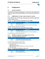
4.3.15

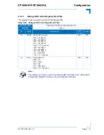
Debug LED Control Register (DLCTRL)

This register is used to switch on and off the Debug LEDs. 

Table 4-20: Debug LED Control Register (LCTRL)

REGISTER NAME

DEBUG LED CONTROL REGISTER (DLCTRL)

ADDRESS

0x291

BIT

NAME

DESCRIPTION

RESET 

VALUE

ACCESS

7-4

DLCMD

Debug LED command:
0000 = Get DLED 0
0001 = Get DLED 1
0010 = Get DLED 2
0011 = Get DLED 3
0100 - 0111 = Reserved
1000 = Set DLED 0
1001 = Set DLED 1
1010 = Set DLED 2
1011 = Set DLED 3
1100 - 1111 = Reserved

0000

R/W

3-0

DLCOL

Debug LED color:
0000 = Off
0001 = Green
0010 = Red
0011 = Red+green
0100 - 1111 = Reserved

0000

R/W

Note ...

This register can only be used if the Debug LEDs indicated in the “Debug LED
Configuration Register” (Table 4-18) are configured in Mode A.

Содержание CP3002-RA

Страница 1: ...embedded it s Kontron User Guide P R E L I M I N A R Y CP3002 RC CP3002 RA 3U CompactPCI Processor Board based on the Intel Core i7 Processor with the Intel QM57 Chipset Doc ID 1039 3625 Rev 1 0 October 8 2010 ...

Страница 2: ...ontron AG All rights reserved All data is for information purposes only and not guaranteed for legal purposes Information has been carefully checked and is believed to be accurate however no responsibility is assumed for inaccuracies Kontron and the Kontron logo and all other trademarks or registered trademarks are the property of their respective own ers and are recognized Specifications are subj...

Страница 3: ...Special Handling and Unpacking Instructions xiii General Instructions on Usage xiv Two Year Warranty xv 1 Introduction 1 3 1 1 Board Overview 1 3 1 2 Board Specific Information 1 4 1 3 System Expansion Capabilities 1 4 1 3 1 Serial ATA Flash Module 1 4 1 4 Board Diagrams 1 4 1 4 1 Functional Block Diagram 1 5 1 4 2 CP3002 RA Front Panel 1 6 1 4 3 Board Layout 1 7 1 5 Technical Specification 1 8 1 ...

Страница 4: ... 5 Gigabit Ethernet Interfaces 2 10 2 10 6 Serial ATA Interface 2 10 2 10 7 GPI and GPO Signals 2 10 2 10 8 Debug Interface 2 10 2 10 9 CompactPCI Bus Interface 2 11 2 10 10 CompactPCI Rear I O Interface 2 11 2 10 10 1 CompactPCI Connectors J1 and J2 2 12 2 10 10 2 CompactPCI Connector Keying 2 12 2 10 10 3 CompactPCI Connectors J1 and J2 Pinouts 2 13 2 10 10 4 Rear I O Pin Description 2 15 2 10 1...

Страница 5: ...ster 1 STAT1 4 6 4 3 3 Control Register 0 CTRL0 4 7 4 3 4 Control Register 1 CTRL1 4 7 4 3 5 Device Protection Register DPROT 4 8 4 3 6 Reset Status Register RSTAT 4 9 4 3 7 Board Interrupt Configuration Register BICFG 4 10 4 3 8 Status Register 2 STAT2 4 11 4 3 9 Board ID High Byte Register BIDH 4 11 4 3 10 Board and PLD Revision Register BREV 4 11 4 3 11 Geographic Addressing Register GEOAD 4 12...

Страница 6: ...2 RC CP3002 RA 5 8 6 Thermal Considerations 6 3 6 1 Board Internal Thermal Monitoring 6 3 6 2 Processor Thermal Monitoring 6 3 6 2 1 Digital Thermal Sensor DTS 6 3 6 2 2 Adaptive Thermal Monitor 6 4 6 2 3 Frequency VID Control 6 4 6 2 4 Clock Modulation 6 4 6 2 5 Catastrophic Cooling Failure Sensor 6 5 6 3 Chipset Thermal Monitor Feature 6 5 6 4 Thermal Characteristics for the CP3002 RC 6 5 6 5 Ex...

Страница 7: ...2 16 2 9 Serial ATA Signal Description 2 17 2 10 USB Signal Description 2 17 2 11 VGA Signal Description 2 17 2 12 GPI GPO Signal Description 2 18 2 13 Power Signal Description 2 18 4 1 JP1 Jumper Setting for RS 422 RXD Termination COMB 4 3 4 2 JP2 Jumper Setting for RS 422 TXD Termination COMB 4 3 4 3 uEFI BIOS Boot Settings Jumper JP3 4 3 4 4 uEFI BIOS Boot Configuration Jumper JP4 4 3 4 5 I O A...

Страница 8: ...m Input Power Voltage Limits 5 3 5 2 DC Operational Input Voltage Ranges 5 3 5 3 CP3002 RC RA in EFI Shell 5 7 5 4 CP3002 RC RA with Win XP and Processor and Graphics in Idle State 5 7 5 5 CP3002 RC RA with Win XP and Typ Proc and Graph Contr Workload 5 7 5 6 CP3002 RC RA with Win XP and Max Processor and Graph Workload 5 7 5 7 Power Consumption of CP3002 RC CP3002 RA Accessories 5 8 5 8 Power Con...

Страница 9: ... Panel 1 6 1 3 CP3002 RC CP3002 RA Board Layout Top View 1 7 1 4 CP3002 RC CP3002 RA Board Layout Bottom View 1 7 2 1 CPCI Connectors J1 J2 2 12 3 1 CP3002 RC with SATA Flash Module 3 9 3 2 CP3002 RA with SATA Flash Module 3 9 6 1 Position of the Reference Points on the CP3002 RC 6 6 6 2 CP3002 RA with i7 620LE 2 0 GHz 6 9 A 1 SATA Flash Module Layout Bottom View A 4 ...

Страница 10: ...Preface CP3002 RC CP3002 RA Page x ID 1039 3625 Rev 1 0 P R E L I M I N A R Y This page has been intentionally left blank ...

Страница 11: ...ent Kontron reserves the right to change modify or improve this document or the product described herein as seen fit by Kontron without further notice Trademarks Kontron the PEP logo and if occurring in this manual CXM are trademarks owned by Kontron Kaufbeuren Germany In addition this document may include names company logos and trademarks which are registered trademarks and therefore proprietary...

Страница 12: ...ing ESD Sensitive Device This symbol and title inform that electronic boards and their compo nents are sensitive to static electricity Therefore care must be taken during all handling operations and inspections of this product in order to ensure product integrity at all times Please read also the section Special Handling and Unpacking Instructions on the following page Warning This symbol and titl...

Страница 13: ...ds or tools This is most easily done by touching a metal part of your system housing It is particularly important to observe standard anti static precautions when changing piggy backs ROM devices jumper settings etc If the product contains batteries for RTC or memory backup ensure that the board is not placed on conductive surfaces including anti static plas tics or sponges They can cause short ci...

Страница 14: ...specific environmental requirements This applies also to the operational temperature range of the specific board version which must not be exceeded If batteries are present their temperature restrictions must be taken into account In performing all necessary installation and application operations please follow only the instructions supplied by the present manual Keep all the original packaging ma...

Страница 15: ...or to refund the original cost of purchase if appropriate In the event of repair re funding or replacement of any part the ownership of the removed or replaced parts reverts to Kontron and the remaining part of the original guarantee or any new guarantee to cover the repaired or replaced items will be transferred to cover the new or repaired items Any exten sions to the original guarantee are cons...

Страница 16: ...Preface CP3002 RC CP3002 RA Page xvi ID 1039 3625 Rev 1 0 P R E L I M I N A R Y This page has been intentionally left blank ...

Страница 17: ...CP3002 RC CP3002 RA Introduction ID 1039 3625 Rev 1 0 Page 1 1 Introduction Chapter 1 1 P R E L I M I N A R Y ...

Страница 18: ...Introduction CP3002 RC CP3002 RA Page 1 2 ID 1039 3625 Rev 1 0 P R E L I M I N A R Y This page has been intentionally left blank ...

Страница 19: ... comes with three Serial ATA interfaces with RAID support one for the SATA Flash module and two on the rear I O as well as one high resolution graphics interface VGA In addition two USB 2 0 ports are available on the rear I O Further interfaces include two serial ports on the rear I O one RS 232 port and one RS 422 RS 232 port The board supports a configurable 32 bit 33 66 MHz PCI CompactPCI inter...

Страница 20: ... 1 5 support One onboard Serial ATA interface Two Serial ATA interfaces on the rear I O Socket for one Serial ATA Flash module SSD Two USB 2 0 ports on the rear I O Two serial ports on the rear I O One RS 232 serial port One RS 422 RS 232 serial port TCG 1 2 compliant Trusted Platform Module TPM on request Two SPI Flash chips for redundant uEFI BIOS Watchdog timer Five general purpose inputs GPI a...

Страница 21: ...R3 w ECC Bank B soldered Intel Core i7 BGA DDR3 DDR3 DMI 1066 MHz SATA Flash Module DMI LPC 2x SATA FDI FDI 2x SATA SATA TPM TPM on request 32 bit 33 66 MHz PCI 4x REQ GNT 2x USB VGA CRT Dual UART SMBus GPIO TTL 2x USB VGA CRT PCIe PCIe x4 x1 Diode Switch Back up Voltage RTC Onboard Power Supplies DC DC etc 2nd uEFI BIOS FLASH RS 232 RS 422 RS 232 COMB RS 422 or RS 232 COMA RS 232 USB Power 2x USB...

Страница 22: ...625 Rev 1 0 P R E L I M I N A R Y 1 4 2 CP3002 RA Front Panel Figure 1 2 CP3002 RA Front Panel Legend Debug LEDs DLED0 red green Debug LED 0 POST DLED1 red green Debug LED 1 POST DLED2 red green Debug LED 2 POST DLED3 red green Debug LED 3 POST 3 2 1 0 ...

Страница 23: ... 3 Board Layout Figure 1 3 CP3002 RC CP3002 RA Board Layout Top View Figure 1 4 CP3002 RC CP3002 RA Board Layout Bottom View GbE Contr J2 J1 Intel Core i7 CPU GMCH Intel QM57 DDR3 Memory J4 1 2 33 34 SATA Flash Module J3 2 1 11 12 DDR3 Memory J6 DLED 0 DLED 1 DLED 2 DLED 3 JP2 JP1 JP4 JP3 ...

Страница 24: ...6 MHz Cache Structure 64 kB L1 cache for each core 32 kB instruction cache 32 kB data cache 256 kB L2 shared instruction data cache for each core 4 MB L3 shared instruction data cache shared between both cores FLASH Memory Two redundant SPI Flash chips 2 x 8 MB for uEFI BIOS Up to 32 GB NAND Flash via an onboard Serial ATA Flash module SSD Serial EEPROM with 64 kbit Chipset Intel QM57 Mobile Intel...

Страница 25: ...ased on the Intel 82580EB Quad Gigabit Ethernet controller Four ports on the rear I O Automatic mode recognition Auto Negotiation Automatic cabling configuration recognition Auto MDI X USB Two USB 2 0 ports on the rear I O interface Serial Two 16C550 compatible UARTs RS 232 RS 422 signaling One RS 232 port on the rear I O COMA One RS 422 RS 232 port on the rear I O COMB Serial ATA Serial ATA Host ...

Страница 26: ...integrated in the Intel QM57 chipset for mon itoring the chipset Specially designed heat sinks Security TPM Trusted Platform Module TPM 1 2 for enhanced hardware and software based data and system security on request Software uEFI BIOS AMI Aptio AMI s next generation BIOS firmware based on the uEFI Specifi cation and the Intel Platform Innovation Framework for EFI LAN boot capability for diskless ...

Страница 27: ...s Back up Voltage A back up voltage input for the RTC can be connected via the rear I O connec tor J2 Climatic Humidity 93 RH at 40 C non condensing acc to IEC 60068 2 78 Dimensions 100 mm x 160 mm Board Weight CP3002 RC 342 g with heat sink but without mezzanine card CP3002 RA 403 g with heat sink but without mezzanine card Table 1 1 CP3002 RC CP3002 RA Main Specifications Continued FEATURES SPEC...

Страница 28: ... Single Shock VITA 47 Class V3 TBD Temperature VITA 47 CC3 VITA 47 CC4 TBD Note Kontron performs comprehensive environmental testing of its products in accor dance with applicable standards Customers desiring to perform further environmental testing of Kontron prod ucts must contact Kontron for assistance prior to performing any such testing This is necessary as it is possible that environmental t...

Страница 29: ...D Single Shock IEC60068 2 27 TBD Permanent Shock IEC60068 2 29 TBD Note Kontron performs comprehensive environmental testing of its products in accor dance with applicable standards Customers desiring to perform further environmental testing of Kontron prod ucts must contact Kontron for assistance prior to performing any such testing This is necessary as it is possible that environmental testing c...

Страница 30: ...A Table 1 4 Related Publications PRODUCT PUBLICATION CompactPCI Systems and Boards CompactPCI Specification PICMG 2 0 Rev 3 0 Kontron CompactPCI Backplane Manual ID 24229 Platform Firmware Unified Extensible Firmware Interface uEFI Specification Version 2 1 All Kontron products Product Safety and Implementation Guide ID 1021 9142 Kontron CP3002 RC CP3002 RA uEFI BIOS User Guide ID 1042 8946 ...

Страница 31: ...CP3002 RC CP3002 RA Functional Description ID 1039 3625 Rev 1 0 Page 2 1 Functional Description Chapter 1 2 P R E L I M I N A R Y ...

Страница 32: ...Functional Description CP3002 RC CP3002 RA Page 2 2 ID 1039 3625 Rev 1 0 P R E L I M I N A R Y This page has been intentionally left blank ...

Страница 33: ...ne execution core to function as two logical processors When this feature is used on the CP3002 RC CP3002 RA four processor cores are present to the operating system This results in higher processing throughput and improved performance on the multithreaded software The Intel Turbo Boost Technology and the Intel Intelligent Power Sharing technology allow the processor and the graphics controller to...

Страница 34: ...ing features Two x4 or eight x1 PCI Express 2 0 ports operating at 2 5 GT s only one x1 PCI Express port is used SATA host controller with six ports 3 Gbit s data transfer rate and RAID 0 1 5 10 support only three ports are used thus only RAID 0 1 5 support is available on the board USB 2 0 host interface with up to 14 USB 2 0 ports available only two ports are used SPI interface support Low Pin C...

Страница 35: ...imer in time results in a system reset or an interrupt In dual stage mode a combination of both interrupt and reset if the Watchdog is not serviced A hardware status flag will be provided to determine if the Watchdog timer generated the reset 2 6 Battery The CP3002 RC CP3002 RA does not include a dedicated battery power source for RTC backup If the board is switched off the RTC will lose its data ...

Страница 36: ... is optimized for embedded systems providing high per formance reliability and security 2 9 Trusted Platform Module 1 2 On Request The CP3002 RC CP3002 RA has been designed to support the Trusted Platform Module TPM 1 2 This feature is available on request TPM1 2 is a security chip specifically designed to provide enhanced hardware and software based data and system security It stores sensi tive d...

Страница 37: ...ocessor overtemperature above 125 C blinking and processor overtemperature above 105 C on green uEFI BIOS POST bit 3 and bit 7 Default Mode B Gigabit Ethernet port D link DLED2 red When lit up during power up it indicates a clock failure Processor overtemperature above 125 C blinking green uEFI BIOS POST bit 2 and bit 6 Default Mode B Gigabit Ethernet port C link DLED1 red When lit up during power...

Страница 38: ... LED2 LED1 LED0 RESULT HIGH NIBBLE off 0 on 1 off 0 off 0 0x4 LOW NIBBLE off 0 off 0 off 0 on 1 0x1 POST CODE 0x41 Note Under normal operating conditions the Debug LEDs should not remain lit during boot up They are intended to be used only for debugging purposes In the event that a Debug LED lights up during boot up and the CP3002 RC CP3002 RA does not boot please contact Kontron If all Debug LEDs...

Страница 39: ...th up to 352 MB memory This technology ensures the most efficient use of all available memory for maximum 3D graphics performance DVMT dynamically responds to application requirements allocating display and texturing memory resources as required 2 10 4 Serial Ports The CP3002 RC CP3002 RA provides two serial ports COMA RS 232 and COMB RS 232 RS 422 both available on the rear I O COMA and COMB are ...

Страница 40: ...rt of Virtual Machines Device queues VMDq per port IEEE 1588 Precision Time Protocol support and per packet timestamp Support of various manageability and power saving features 2 10 6 Serial ATA Interface The CP3002 RC CP3002 RA provides three SATA I 1 5 Gbit sec and SATA II 3 0 Gbit sec compliant interfaces with RAID support 0 1 5 One interface is used for the SATA Flash mod ule and two SATA inte...

Страница 41: ...es the following interfaces all signals are available on J2 One COMA port RS 232 signaling no buffer on the rear I O module RTM is necessary One COMB port RS 232 RS 422 signaling no buffer on the rear I O module is neces sary Two USB 2 0 port One VGA analog port Four Gigabit Ethernet ports magnetics on the rear I O module are necessary Two SATA ports Five GPIs and three GPOs TTL signaling Back up ...

Страница 42: ...ctPCI standard is electrically identical to the PCI local bus However these systems are enhanced to operate in rugged industrial environments and to support multiple slots 2 10 10 2 CompactPCI Connector Keying CompactPCI backplane connectors support guide lugs to ensure a correct polarized mating 3 3 V or 5 V V I O coding The CP3002 RC CP3002 RA supports universal 3 3 V and 5 V PCI V I O signaling...

Страница 43: ...3 3V AD 6 AD 5 GND 21 NC 3 3V AD 9 AD 8 M66EN C BE 0 GND 20 NC AD 12 GND V I O AD 11 AD 10 GND 19 NC 3 3V AD 15 AD 14 GND AD 13 GND 18 NC SERR GND 3 3V PAR C BE 1 GND 17 NC 3 3V IPMB SCL IPMB SDA GND PERR GND 16 NC DEVSEL PCIXCAP V I O STOP LOCK GND 15 NC 3 3V FRAME IRDY BDSEL TRDY GND 12 14 Key Area 11 NC AD 18 AD 17 AD 16 GND C BE 2 GND 10 NC AD 21 GND 3 3V AD 20 AD 19 GND 9 NC C BE 3 NC AD 23 G...

Страница 44: ..._DA lPA_DA RSVD lPA_DC lPA_DC GND 11 NC lPA_DB lPA_DB COMA_RI lPA_DD lPA_DD GND 10 NC GND GND VGA_RED COMA_DSR GND GND 9 NC SATA0TX COMA_RXD VGA_HSYNC COMB_RX RXD SATA1TX GND 8 NC SATA0TX COMA_CTS VGA_BLUE COMB_RX CTS SATA1TX GND 7 NC GND GND VGA_DDC_DATA GND GND GND 6 NC SATA0RX COMA_RTS VGA_GREEN COMB_TX RTS SATA1RX GND 5 NC SATA0RX COMA_TXD VGA_VSYNC COMB_TX TXD SATA1RX GND 4 NC VI O 5V VGA_DDC...

Страница 45: ...R DSR signal serial port COMA RTM RS 232 level D4 COMA_DCD DCD signal serial port COMA RTM RS 232 level E4 COMA_DTR DTR signal serial port COMA CP3002 RC RA RS 232 level C11 COMA_RI RI signal serial port COMA RTM RS 232 level D5 COMB_TX TXD TXD serial port COMB CP3002 RC RA RS 232 level TX serial port COMB CP3002 RC RA RS 422 level D9 COMB_RX RXD RXD serial port COMB RTM RS 232 level RX serial por...

Страница 46: ...14 IPB_DC Media dependent interface port B Bidirectional Analog D13 IPB_DD Media dependent interface port B Bidirectional Analog E13 IPB_DD Media dependent interface port B Bidirectional Analog A18 IPC_DA Media dependent interface port C Bidirectional Analog B18 IPC_DA Media dependent interface port C Bidirectional Analog A17 IPC_DB Media dependent interface port C Bidirectional Analog B17 IPC_DB ...

Страница 47: ...tial Table 2 10 USB Signal Description PIN on J2 SIGNAL FUNCTION DRIVEN BY SIGNALING VOLTAGE D21 USB0 Positive USB port 0 Bidirectional Differential D20 USB0 Negative USB port 0 Bidirectional Differential E20 USB0_PWR_5V USB power supply 5 V port 0 CP3002 RC RA 5 V C21 USB1 Positive USB port 1 Bidirectional Differential C20 USB1 Negative USB port 1 Bidirectional Differential E21 USB1_PWR_5V USB po...

Страница 48: ... GPI0 General purpose input 0 RTM LVTTL 3 3 V A3 GPI1 General purpose input 1 RTM LVTTL 3 3 V D19 GPI2 General purpose input 2 RTM LVTTL 3 3 V D3 GPI3 General purpose input 3 RTM LVTTL 3 3 V A21 GPI4 General purpose input 4 RTM LVTTL 3 3 V C18 GPO0 General purpose output 0 CP3002 RC RA LVTTL 3 3 V A20 GPO1 General purpose output 1 CP3002 RC RA LVTTL 3 3 V E3 GPO2 General purpose output 2 CP3002 RC...

Страница 49: ...CP3002 RC CP3002 RA Installation ID 1039 3625 Rev 1 0 Page 3 1 Installation Chapter 1 3 P R E L I M I N A R Y ...

Страница 50: ...Installation CP3002 RC CP3002 RA Page 3 2 ID 1039 3625 Rev 1 0 P R E L I M I N A R Y This page has been intentionally left blank ...

Страница 51: ... container until such time as the board and heat sink have cooled down to room temperature Caution If your board type is not specifically qualified as being hot swap capable switch off the CompactPCI system power before installing the board in a free CompactPCI slot Failure to do so could endanger your life or health and may damage your board or system Note Certain CompactPCI boards require bus ma...

Страница 52: ...ax the wedge lock turn the wedge lock s screw counter clockwise using a 2 5 mm hex key until the screw is against the stop The screw should turn lightly If when turning the screw perceptible resistance is encountered it is at the stop Do not apply more force than necessary 4 Carefully insert the board into the slot designated by the application requirements for the board until it makes contact wit...

Страница 53: ... appropriate CP3002 RC specific software application and system docu mentation Note The chassis of ruggedized systems do not necessarily provide an objec tive means of determining when the board is properly seated in the back plane During insertion it is possible however to sense when the board gives way and seats into the connector At this point the application of more force does not result in fu...

Страница 54: ... s screw counter clockwise using a 2 5 mm hex key until the screw is against the stop 5 Disengage the board from the backplane using the ejector handle as required until the board is disengaged from the backplane 6 After disengaging the board from the backplane pull the board out of the slot 7 Ensure that the ejector handle retaining screw is properly fastened 8 Dispose of the board as required Wa...

Страница 55: ...ot designated by the application requirements for the board until it makes contact with the backplane connectors Warning The CP3002 RA provides no ESD discharge strips Always ensure that the CP3002 RA is discharged prior to installation in a CompactPCI back plane Failure to comply with this instruction may cause damage to the board or result in improper system operation Warning On the CP3002 RA th...

Страница 56: ...e board ejection handle and then by pressing the handle as required until the board is disengaged 5 After disengaging the board from the backplane pull the board out of the slot 6 Dispose of the board as required 3 6 Hot Swap Procedures The CP3002 RC CP3002 RA is not designed for hot swap operation Do not attempt the hot swap this board However the CP3002 RC CP3002 RA supports the addition or remo...

Страница 57: ...002 RC CP3002 RA Installation ID 1039 3625 Rev 1 0 Page 3 9 P R E L I M I N A R Y Figure 3 1 CP3002 RC with SATA Flash Module Figure 3 2 CP3002 RA with SATA Flash Module SATA Flash Module SATA Flash Module ...

Страница 58: ...t and all other onboard peripheral drivers is described in detail in the relevant Driver Kit files Installation of an operating system is a function of the OS software and is not addressed in this manual Refer to appropriate OS software documentation for installation Note Only qualified SATA Flash modules from Kontron are authorized for use with the CP3002 RC CP3002 RA Failure to comply with the a...

Страница 59: ...CP3002 RC CP3002 RA Configuration ID 1039 3625 Rev 1 0 Page 4 1 Configuration Chapter 1 4 P R E L I M I N A R Y ...

Страница 60: ...Configuration CP3002 RC CP3002 RA Page 4 2 ID 1039 3625 Rev 1 0 P R E L I M I N A R Y This page has been intentionally left blank ...

Страница 61: ... 2 uEFI BIOS Configuration Jumper Settings JP3 and JP4 The default setting is indicated by using italic bold To clear the uEFI BIOS settings proceed as follows 1 Close jumper JP3 2 Apply power to the system 3 After successful boot from uEFI BIOS remove power from the system 4 Open jumper JP3 Table 4 1 JP1 Jumper Setting for RS 422 RXD Termination COMB JP1 DESCRIPTION Open RXD termination inactive ...

Страница 62: ...us Register 0 STAT0 0x281 Status Register 1 STAT1 0x282 Control Register 0 CTRL0 0x283 Control Register 1 CTRL1 0x284 Device Protection Register DPROT 0x285 Reset Status Register RSTAT 0x286 Board Interrupt Configuration Register BICFG 0x287 Status Register 2 STAT2 0x288 Board ID High Byte Register BIDH 0x289 Board and PLD Revision Register BREV 0x28A Geographic Addressing Register GEOAD 0x28B Res...

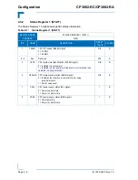
Страница 63: ...he system uEFI BIOS may be relying on the state of the bits under its control Table 4 6 Status Register 0 STAT0 REGISTER NAME STATUS REGISTER 0 STAT0 ADDRESS 0x280 BIT NAME DESCRIPTION RESET VALUE ACCESS 7 Res Reserved 0 R 6 BBEI uEFI BIOS boot end indication 0 uEFI BIOS is booting 1 uEFI BIOS boot is finished 1 R 5 4 BFSS Boot Flash selection status 00 Primary boot Flash active 01 Secondary boot ...

Страница 64: ...3 MHz 1 66 MHz N A R 6 4 Res Reserved 000 R 3 CSYS CPCI system slot identification SYSEN signal 0 Installed in a system slot 1 Installed in a peripheral slot the board is not intended to be operated in a peripheral slot N A R 2 CENUM CPCI system enumeration ENUM signal 0 Indicates the insertion or removal of a hot swap peripheral board 1 No hot swap event N A R 1 CFAL CPCI power supply status FAL ...

Страница 65: ...ection 0 Select default boot Flash for update 1 Select alternative boot Flash for update 0 R W 3 2 CPMC2 COMB port mode configuration 00 RS 232 mode 01 RS 422 mode 10 Reserved 11 Reserved 01 R W 1 0 Res Reserved 00 R Table 4 9 Control Register 1 CTRL1 REGISTER NAME CONTROL REGISTER 1 CTRL1 ADDRESS 0x283 BIT NAME DESCRIPTION RESET VALUE ACCESS 7 SRST SATA Flash module configuration 0 Reset of SATA ...

Страница 66: ...served 00000 R 2 SFWP SATA Flash module write protection 0 SATA Flash module not write protected 1 SATA Flash module write protected Writing a 1 to this bit sets the bit If this bit is set it cannot be cleared 0 R W 1 EEWP EEPROM write protection 0 EEPROM not write protected 1 EEPROM write protected Writing a 1 to this bit sets the bit If this bit is set it cannot be cleared 0 R W 0 BFWP Boot Flas...

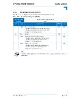
Страница 67: ...ftware warm reset 1 System reset generated by power on cold reset Writing a 1 to this bit clears the bit N A R W 6 2 Res Reserved 00000 R 1 CPRS CompactPCI reset status PRST signal 0 System reset not generated by CPCI reset input 1 System reset generated by CPCI reset input Writing a 1 to this bit clears the bit 0 R W 0 WTRS Watchdog timer reset status 0 System reset not generated by Watchdog time...

Страница 68: ...FG ADDRESS 0x286 BIT NAME DESCRIPTION RESET VALUE ACCESS 7 UICF UART IRQ3 and IRQ4 interrupt configuration 0 Disabled 1 Enabled 1 R W 6 CFICF CPCI fail signal interrupt configuration FAL signal 0 IRQ5 disabled 1 IRQ5 enabled 0 R W 5 CEICF CPCI enumeration signal interrupt configuration ENUM signal 0 IRQ5 disabled 1 IRQ5 enabled 0 R W 4 CDICF CPCI derate signal interrupt configuration DEG signal 0 ...

Страница 69: ...vice PLD require different handling by the software It starts with the value 0x00 and will be incremented with each change in hardware as development continues Table 4 13 Status Register 2 STAT2 REGISTER NAME STATUS REGISTER 2 STAT2 ADDRESS 0x287 BIT NAME DESCRIPTION RESET VALUE ACCESS 7 6 Res Reserved 00 R 5 4 RCFG Rear I O configuration 00 Reserved 01 COMA COMB GPIO 10 Reserved 11 Reserved 01 R ...

Страница 70: ...eographic Addressing Register GEOAD This register holds the CompactPCI geographic address Table 4 16 Geographic Addressing Register GEOAD REGISTER NAME GEOGRAPHIC ADDRESSING REGISTER GEOAD ADDRESS 0x28A BIT NAME DESCRIPTION RESET VALUE ACCESS 7 5 Res Reserved 000 R 4 0 GA Geographic address N A R ...

Страница 71: ...d as follows Timer only mode In this mode the Watchdog is enabled using the required timeout period Nor mally the Watchdog is retriggered by writing a 1 to the WTR bit In the event a timeout occurs the WTE bit is set to 1 This bit can then be polled by the application and handled accordingly To continue using the Watchdog write a 1 to the WTE bit and then retrigger the Watchdog using WTR The WTE b...

Страница 72: ...mode 00 R W 4 WEN WTR Watchdog enable Watchdog trigger control bit 0 Watchdog timer not enabled Prior to the Watchdog being enabled this bit is known as WEN After the Watchdog is enabled it is known as WTR Once the Watchdog timer has been enabled this bit cannot be reset to 0 As long as the Watchdog timer is enabled it will indicate a 1 1 Watchdog timer enabled Writing a 1 to this bit causes the W...

Страница 73: ... type identifier in the form of a hexadecimal number The Board ID Low Byte Register is located in the address 0x28D The Board ID High Byte Register is located in the address 0x288 Table 4 18 Board ID Low Byte Register BIDL REGISTER NAME BOARD ID LOW BYTE REGISTER BIDL ADDRESS 0x28D BIT NAME DESCRIPTION RESET VALUE ACCESS 7 0 BIDL Board identification CP3002 RC CP3002 RA 0xB330 30 R ...

Страница 74: ...ug LED 1 controlled by host green red DLED0 Debug LED 0 controlled by host green red 3 Configured for Mode B the Debug LEDs are dedicated to functions as follows DLED3 Gigabit Ethernet port D link status green DLED2 Gigabit Ethernet port C link status green DLED1 Gigabit Ethernet port B link status green DLED0 Gigabit Ethernet port A link status green Beside the configurable functions described ab...

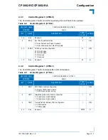
Страница 75: ... 0x291 BIT NAME DESCRIPTION RESET VALUE ACCESS 7 4 DLCMD Debug LED command 0000 Get DLED 0 0001 Get DLED 1 0010 Get DLED 2 0011 Get DLED 3 0100 0111 Reserved 1000 Set DLED 0 1001 Set DLED 1 1010 Set DLED 2 1011 Set DLED 3 1100 1111 Reserved 0000 R W 3 0 DLCOL Debug LED color 0000 Off 0001 Green 0010 Red 0011 Red green 0100 1111 Reserved 0000 R W Note This register can only be used if the Debug LED...

Страница 76: ...RIPTION RESET VALUE ACCESS 7 3 Res Reserved 00000 R 2 GPO2 General Purpose Output 2 0 Output low 1 Output high 0 R W 1 GPO1 General Purpose Output 1 0 Output low 1 Output high 0 R W 0 GPO0 General Purpose Output 0 0 Output low 1 Output high 0 R W Table 4 22 General Purpose Input Register GPIN REGISTER NAME GENERAL PURPOSE INPUT REGISTER GPIN ADDRESS 0x293 BIT NAME DESCRIPTION RESET VALUE ACCESS 7 ...

Страница 77: ...CP3002 RC CP3002 RA Power Considerations ID 1039 3625 Rev 1 0 Page 5 1 Power Considerations Chapter 1 5 P R E L I M I N A R Y ...

Страница 78: ...Power Considerations CP3002 RC CP3002 RA Page 5 2 ID 1039 3625 Rev 1 0 P R E L I M I N A R Y This page has been intentionally left blank ...

Страница 79: ... ed Power supplies to be used with the CP3002 RC CP3002 RA should be carefully tested to ensure compliance with these ratings The following table specifies the ranges for the different input power voltages within which the board is functional The CP3002 RC CP3002 RA is not guaranteed to function if the board is not operated within the prescribed limits Table 5 1 Maximum Input Power Voltage Limits ...

Страница 80: ...s the design of the CP3002 RC CP3002 RA has been optimized for minimal power consump tion the power supply unit shall be stable even without minimum load Where possible power supplies which support voltage sensing should be used Depending on the system configuration this may require an appropriate backplane The power supply should be sufficient to allow for backplane input line resistance variatio...

Страница 81: ... the 5 V begins to decrease all other input voltages must decrease accordingly This is required in order to preclude cross currents within the CP3002 RC CP3002 RA Failure to comply with above may result in damage to the board or improper system operation Note If the main power input is switched off the supply voltages will not go to 0 V instantly It will take a couple of seconds until the capacito...

Страница 82: ...ent enabled and the graphics controller was in idle state no application running CP3002 RC CP3002 RA with Windows XP 32 bit processor and graphics controller in idle state For this measurement all processor cores and the graphics controller were in idle state power management enabled and no application running CP3002 RC CP3002 RA with Win XP 32 bit typical processor and graphics controller workloa...

Страница 83: ...Win XP and Processor and Graphics in Idle State POWER typ Intel Core i7 620LE LV 2 0 GHz 5 V 4 0 W 3 3 V 7 0 W Total 11 0 W Table 5 5 CP3002 RC RA with Win XP and Typ Proc and Graphics Controller Workload POWER typ Intel Core i7 620LE LV 2 0 GHz 5 V 21 0 W 3 3 V 10 0 W Total 31 0 W Table 5 6 CP3002 RC RA with Win XP and Max Processor and Graphics Workload POWER typ Intel Core i7 620LE LV 2 0 GHz 5...

Страница 84: ...s been applied power on For further information on the start up current please contact Kontron Table 5 7 Power Consumption of CP3002 RC CP3002 RA Accessories MODULE POWER 5 V POWER 3 3 V Keyboard approx 0 1 W DDR3 SDRAM update from 4 GB to 8 GB approx 1 0 W SATA Flash module approx 0 5 W Table 5 8 Power Consumption of the Gigabit Ethernet Controller ETHERNET PORT POWER 5 V POWER 3 3 V Intel 82580E...

Страница 85: ...CP3002 RC CP3002 RA Thermal Considerations ID 1039 3625 Rev 1 0 Page 6 1 Thermal Considerations Chapter 1 6 P R E L I M I N A R Y ...

Страница 86: ...Thermal Considerations CP3002 RC CP3002 RA Page 6 2 ID 1039 3625 Rev 1 0 P R E L I M I N A R Y This page has been intentionally left blank ...

Страница 87: ...ocessor must remain within the maximum die temperature specifications The max imum die temperature for Intel Core i7 610E and i7 620LE multi chip processors is as fol lows Processor die 105 C Graphics and memory controller die 100 C The Intel Core i7 processor uses the Adaptive Thermal Monitor feature to protect the pro cessor from overheating and includes the following on die temperature sensors ...

Страница 88: ... to Intel Thermal Monitor 2 TM2 in previous generation processors Running the processor at the lower frequency and voltage will reduce power consumption and should allow the processor to cool off If the processor temperature does not drop below the TCC activation point a second frequency and voltage transition will take place This sequence of temperature checking and Frequency VID reduction will c...

Страница 89: ...se temperature is 111 C 6 4 Thermal Characteristics for the CP3002 RC The thermal concept of the CP3002 RC is based on a specially designed full board heat spreader and wedge lock clamping mechanisms The heat spreader provides optimal heat transfer to the board s top and bottom edges as well as enhanced structural support for ruggedized environments The wedge locks serve two functions First they p...

Страница 90: ...ENCE POINT TEMPERATURE AT 105 C CPU DIE TEMPERATURE CPU VERSION MAXIMUM PROCESSOR AND GRAPHICS CONTROLLER WORKLOAD TYPICAL PROCESSOR AND GRAPHICS CONTROLLER WORKLOAD Point 1 Point 2 Point 1 Point 2 Intel Core i7 620LE 2 0 GHz 80 C 80 C 85 C 85 C Note The temperature values indicated in the tables above can vary depending on the location of the measurement point or the system performance Warning As...

Страница 91: ...l aspect One diagram per CPU version and ruggedization level is provided There are up to two curves representing upper level work ing points based on different levels of average CPU utilization When operating below the cor responding curve the CPU runs steadily without any intervention of thermal supervision When operated above the corresponding curve various thermal protection mechanisms may take...

Страница 92: ... this operating point thermal supervision will become active protecting the CPU from thermal destruction The minimum airflow rate provided must be more than the value specified in the diagram Volumetric flow rate The volumetric flow rate refers to an airflow through a fixed cross sectional area i e slot width x depth The volumetric flow rate is specified in m h cubic meter per hour or cfm cubic fe...

Страница 93: ... requirements to comply with operational environment conditions In most cases this will lead to a reduction in the maximum allowable ambient operating temperature or even re quire active cooling of the operating environment Warning As Kontron assumes no responsibility for any damage to the CP3002 RC CP3002 RA or other equipment resulting from overheating of the CPU it is highly recommended that sy...

Страница 94: ...Thermal Considerations CP3002 RC CP3002 RA Page 6 10 ID 1039 3625 Rev 1 0 P R E L I M I N A R Y This page has been intentionally left blank ...

Страница 95: ...CP3002 RC CP3002 RA SATA Flash Module ID 1039 3625 Rev 1 0 Page A 1 SATA Flash Module Appendix 1 A P R E L I M I N A R Y ...

Страница 96: ...SATA Flash Module CP3002 RC CP3002 RA Page A 2 ID 1039 3625 Rev 1 0 P R E L I M I N A R Y This page has been intentionally left blank ...

Страница 97: ...hnical Specifications Note Write protection is available for this module Please contact Kontron for further assistance if write protection is required Table A 1 SATA Flash Module Specifications SATA FLASH MODULE SPECIFICATIONS Interface Board to Board Connector One 34 pin male board to board connector J1 Memory Memory Up to 32 GB SLC based NAND Flash memory Built in full hard disk emulation Up to ...

Страница 98: ...39 3625 Rev 1 0 P R E L I M I N A R Y A 2 SATA Flash Module Layout The SATA Flash module includes one board to board connector J1 for connection to the CP3002 RC CP3002 RA Figure A 1 SATA Flash Module Layout Bottom View NAND Flash NAND Flash J1 33 1 2 34 ...

Отзывы: