background image

UX-M3R

1-5

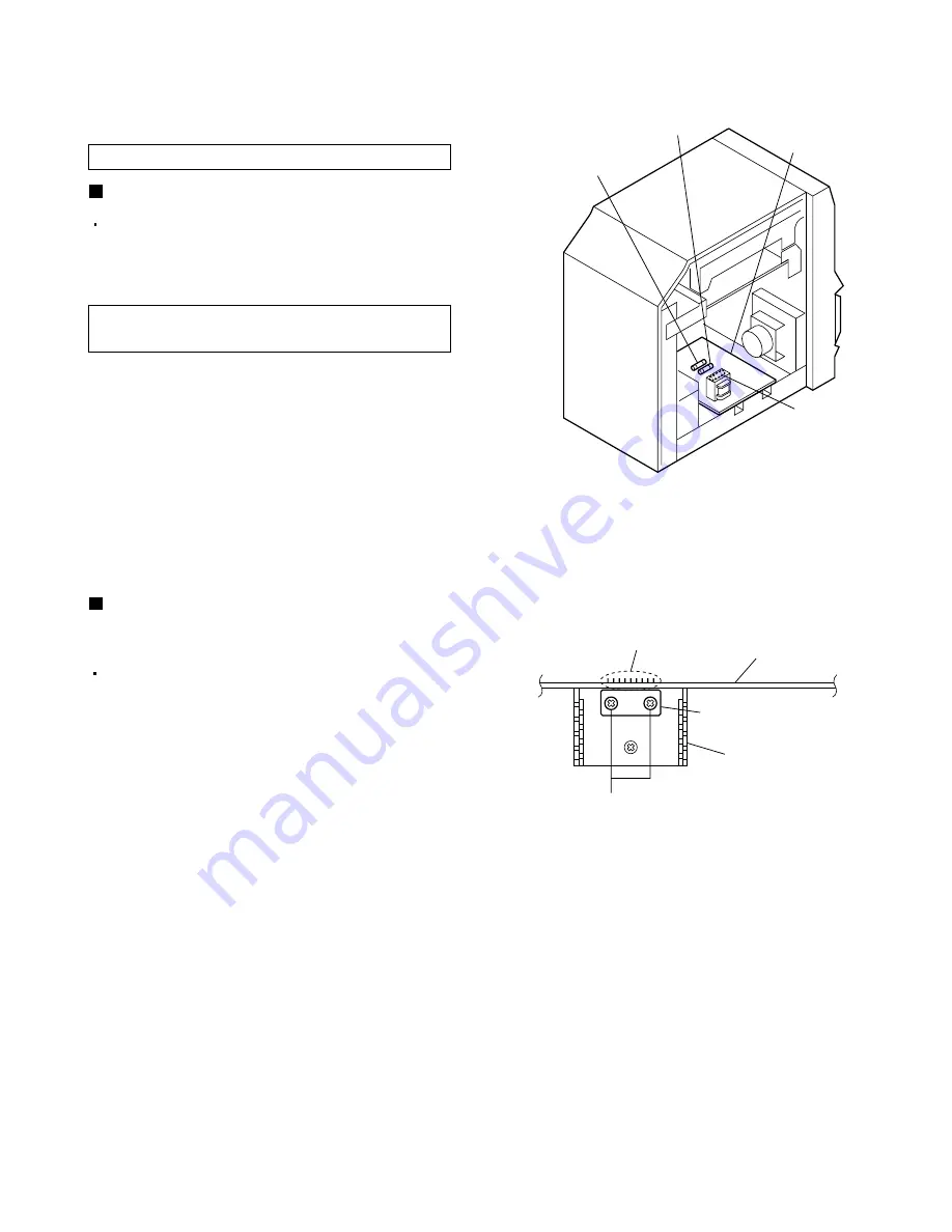
Fuse(F903)

1A 250V

Fuse(F901)

1A 250V

Heat sink

Soldered part 

a

A

Power board

Fuse(F902)

2A 250V

Fig.1

Fig.2

Main board

Power amplifier IC

(IC401)

Replacing the fuses            (See Fig. 1.)

<Main body section>

Remove the left side panel according to its 
disassembly method (see 

Figs. 5

 and 

6

).

Fuses are located inside the left side panel.

Disassembly method

Replacement of the fuses and power amplifier IC

[Caution]  Be sure to replace the required fuses
                  with designated ones.

Replacing the power amplifier IC on 

the main board                    (See Fig. 2.)

1.

2.

Remove the main board according to its 
disassembly method (see Figs. 

17

 and 

18

).

Remove the two screws 

A

 that attach the power 

amplifier IC onto the heat sink.

In order to replace the power amplifier IC, remove 
the solder from soldered part 

a

 on the back side of 

the main board.

Содержание UX-M3R

Страница 1: ...ons UX M3R Area suffix B U K E Continental Europe EN Northern Europe EV Eastern Europe SP UXM3 CA UXM3R SP UXM3 DISPLAY MODE PHONES PROGRAM REC STOP CLEAR PLAY PAUSE PRE EQ HBS VOLUME REPEAT SEARCH TUNING RANDOM CD TUNER TAPE BAND M I C R O C O M P O N E N T S Y S T E M U X M 3 R FULL LOGIC DECK CD SYNCHRO RECORDING TIMER ON OFF SET REMAIN RDS MODE EJECT INTRO RDS SEARCH PRESET OPEN CLOSE STANDBY ...

Страница 2: ...uct antenna terminals knobs metal cabinet screw heads headphone jack control shafts etc to be sure the product is safe to operate without danger of electrical shock Do not use a line isolation transformer during this check Plug the AC line cord directly into the AC outlet Using a Leakage Current Tester measure the leakage current from each exposed metal parts of the cabinet particularly any expose...

Страница 3: ...icity Ground the workbench by laying conductive material such as a conductive sheet or an iron plate over it before placing the traverse unit optical pickup on it 2 1 Ground the workbench 2 2 Ground yourself Use an anti static wrist strap to release any static electricity built up in your body In order to maintain quality during transport and before installation both sides of the laser diode on th...

Страница 4: ...es malfunction the laser is able to function 6 CAUTION Use of controls adjustments or performance of procedures other than those specified herein may result in hazardous radiation exposure VARNING Osynlig laserstrålning är denna del är öppnad och spårren är urkopplad Betrakta ej strålen VARO Avattaessa ja suojalukitus ohitettaessa olet alttiina näkymättömälle lasersäteilylle Älä katso säteeseen AD...

Страница 5: ...d inside the left side panel Disassembly method Replacement of the fuses and power amplifier IC Caution Be sure to replace the required fuses with designated ones Replacing the power amplifier IC on the main board See Fig 2 1 2 Remove the main board according to its disassembly method see Figs 17 and 18 Remove the two screws A that attach the power amplifier IC onto the heat sink In order to repla...

Страница 6: ...toward the rear in the direction of arrow 1 until the claw b at the back of the panel is hooked by the chassis and then lift the panel upward in the direction of arrow 2 to remove it Removing the left side panel See Figs 5 and 6 1 2 From the left side of the main body remove the three screws B and three screws C retaining the left side panel Slide the left side panel toward the rear in the directi...

Страница 7: ...board Disconnect the wire from the connector on the cassette switch board Remove the screw E retaining the bracket on the ear phone board Disconnect the wires from the two connectors CN201 and CN402 on the main board Disconnect the wires from the two connectors CN607 and CN608 on the CD MCU board Remove the four screws F and the two screws G retaining the bracket of the CD mechanism assembly from ...

Страница 8: ...move the top cover Remove the front panel assembly Disconnect the wires from the four connectors CN601 CN602 CN603 and CN701 on the CD MCU board From the left side of the main body remove the tie band bundling the wires Loosen the screw J retaining the main board From the left and right sides of the main body remove the four screws K retaining the bracket Slide the CD mechanism assembly toward the...

Страница 9: ...s Remove the power board by pinching the two studs retaining the board using radio pliers etc Removing the main board See Figs 17 and 18 1 2 3 4 Remove the left and right side panels Remove the top cover Remove the front panel assembly Remove the CD mechanism assembly Remove the two screws M retaining the speaker terminal of the main board From the top side of the main body remove the screw N reta...

Страница 10: ... the front panel assembly Take out the cassette door from the back side of the front panel assembly Remove the left and right side panels Remove the top cover Remove the front panel assembly Remove the cassette mechanism assembly Remove the cassette door cover Caution After assembly apply a locking agent to the screws Q and R Front panel assembly section Removing the cassette mechanism assembly Se...

Страница 11: ...he CD MCU board and take out the CD MCU board Caution Be sure to solder the short land part n on the CD pickup unit before disconnecting the card wire from the CD pickup assembly see Fig 24 If the card wire is disconnected without attaching solder the CD pickup may be destroyed by static electricity In the assembly be sure to remove solder from the short land part n after connecting the card wire ...

Страница 12: ...op of the CD mechanism assembly push the section r of the elevator in the direction of the arrow and lower the CD pickup assembly Pull out the tray While opening up the claws s at the left and right of the tray in the directions of the arrows remove the tray While pushing the claw t on the CD mechanism assembly downwards slide the elevator fully in the direction of the arrow Remove the transparent...

Страница 13: ... Remove the slit washer retaining the feed middle gear and take out the feed middle gear Remove the two screws Y retaining the shaft Turn the CD pickup unit upside down and apply solder to the short land part n Disconnect the card wire from the CD pickup unit and replace the unit Note Use the following procedure to replace only the CD pickup unit Caution Be sure to solder the short land part n on ...

Страница 14: ...est tape VT712 For tape speed and wow flutter VT724 For reference level VT703 For playback frequency VT703 For head azimuth adjustment 13 Blank tape TAPE AC 225 Measurement conditions Power supply voltage AC230V 50Hz Measuring instruments Radio section FM 1kHz 22 5kHz deviation FM STEREO 1kHz 67 5kHz deviation pilot signal 7 5kHz AM 1kHz 30 modulation Reference output H phone output 10dBs 0 245V 3...

Страница 15: ...point P207 is 68kHz 1kHz if not adjust L203 until the frequency counter indicates 68 kHz 1kHz Tape Normal Signal output terminal Cassette REC PLAY HEAD Bias frequency check L203 P207 See Fig 3 on page 1 16 At TUNER set the BAND to the FM position and record the reference 1kHz signal and 8kHz signal alternately repeatedly While playing back the recorded signal of the 1kHz signal differ from that of...

Страница 16: ...SSETTE MOTOR Tape Speed Adj Location of adjusting parts Cassette mechanism section Fig 2 Main board TA2104 FM OSC P102 FM VT FM RF FM RF AM RF AM RF AM IF BIAS FREQUENCY ADJ P207 BIAS FREQUENCY P101 AM VT FM ANT AM ANT AM OSC CN101 L101 TC101 L106 L105 IC101 TC102 L102 T101 L203 Fig 3 ...

Страница 17: ...point Turn on focus servo Disc spinning Radial_error scaling Check that the voltage at the pin1 and pin2 of CN703 is 0 65V Before connecting a measuring instrument to the measuring point turn the power of the main unit to OFF After performing a measurement and before disconnecting the measuring instrument again turn the power of the main unit to OFF If a measuring instrument is disconnected while ...

Страница 18: ...hen the life of the laser diode has expired the following symptoms will appear The level of RF output EFM output ampli tude of eye pattern will below Is the level of RF OUT under 1 25V 0 22Vp p Replace it NO YES O K 3 Semi fixed resistor on the APC PC board The semi fixed resistor on the APC printed circuit board which is attached to the pickup is used to adjust the laser power Since this adjustme...

Страница 19: ...01 Defective IC102 Intermediate frequency tuning faulty Poor contact in FM antenna circuit No sound weak sound Low sensitivity FM Connect the built in or external antenna Replace or repair the switch Check voltages Replace if necessary Check voltages Replace if necessary Readjust see Adjustment method Resolder or repair as required Dirty capstan or head Irregular cassette tape winding Defective IC...

Страница 20: ...n No Symbol I O Function 28 29 30 31 32 33 34 35 36 37 38 39 40 41 42 43 44 45 46 47 48 49 50 51 52 91 92 95 96 97 98 99 100 B PHOTO OUTPUT CD RW RES CCE BUCK BUS0 BUS1 BUS2 BUS3 TRAY IN SLOUT TRAY OUT SLIN SLT CLT SLEND NC RDS DATA STEREO PWR DET AD K3 AD K2 AD K1 VAREF BOOT VSS VDD SEG39 0 COM3 0 VLC PLL DATA PLL CLK PLL PRD VDD Reel pulse input of deck B Have pulse input means the tape is rotat...

Страница 21: ...l output the text data with serial by command I O O O O O O O O O O I O O O O O O O O 80 51 1 30 100 81 31 50 23 24 25 26 27 28 29 30 31 32 33 34 35 36 37 38 39 40 41 42 43 44 45 46 47 48 49 50 VDD2 TESIO0 P2VREF HSSW ZDET PDO TMAXS TMAX LPFN LPFO PVREF VCOREF VCOF AVSS1 SLCO RFI AVDD1 RFCT RFZI RFRP FEI SBAD TSIN TEI TEZI FOO TRO VREF Digital power supply voltage terminal Test input output termin...

Страница 22: ...of 2 state PWM Normally keep at open DAC test mode terminal Normally keep at open O O O O O O O O O O I O I O I O I O I I I 71 72 73 74 75 76 77 78 79 80 81 82 83 84 85 86 87 88 89 90 91 92 93 94 95 96 97 98 99 100 TESIN TESIO1 VSS4 PXI PXO VDD4 XVSS XI XO XVDD DVSR RO DVDD DVR LO DVSL TEST1 TEST2 TEST3 BUS0 BUS1 BUS2 BUS3 VDD5 VSS5 BUCK CCE TEST4 TSMOD RST Test input terminal Normally keep at L l...

Страница 23: ...ation Ch 2 Output Ch 2 ALC input Ch 2 Ripple filter Vcc 1 2 3 4 5 6 7 8 9 10 11 12 13 14 I O I I I I O I GND ALC time constant by resistance and capacitor Right channel ALC input Right channel output No connect Right channel negative feed back input Right channel signal input Left channel signal input Left channel negative feed back input No connect Left channel output Left channel ALC input Rippl...

Страница 24: ...2 3 4 5 6 7 8 9 10 11 12 NF1 IN1 RIPPLEFILTER PREGND IN2 NF2 OUT2 MUTE POWERGND2 Vcc OUT1 POWERGND1 Right channel negative feed back Right channel signal input Ripple filter PRE GND Left channel signal input Left channel negative feed back Left channel output Mute control Power GND Power supply Right channel output Power GND PIN No Symbol I I O O I O Function 2 Pin function 1 2 3 4 5 6 7 8 OUT1 IN...

Страница 25: ...der signal output terminal Focus error signal output terminal FE amplifier negative input terminal Reference voltage Vref output terminal Vref 2 1V when Vcc 5V Track count signal output terminal RFRP detect circuit input terminal RF gain signal output terminal RF amplitude adjustment control signal input terminal controlled by 3 PWM signal PWM carrier 88 2 kHz RF signal amplitude adjustment amplif...

Страница 26: ...X STMONO Crystal oscillator pins Crystal oscillator pins Period signal input Clock signal input Serial data input output General purpose output port General purpose output port General purpose output port General purpose output port General purpose I O port PIN No Symbol 11 12 13 14 15 16 17 18 19 20 General purpose I O port Power supply pin Programmable counter input Programmable counter input Gr...

Страница 27: ...h Audio signal input pin R ch Audio signal input pin R ch Audio signal input pin R ch Audio signal input pin R ch Power supply voltage pin I I I I O I I I I O I I I I I I O I I I I O I I I I 3 Pin Function GND L IN1 L IN2 L IN3 L IN4 L SW OUT L VR IN L B1 L B2 L B3 L TONE OUT L T1 Vref CK VDD R IN1 R IN2 R IN3 R IN4 R SW OUT R VR IN R B1 R B2 R B3 R TONE OUT R T1 STB DATA 28 27 26 25 24 23 22 21 2...

Страница 28: ...Supply terminal of output stage for CH4 Inverted output for CH4 Power GND O O I I O O O O I I O O 2 Pin Function PW GND1 OUT 1 PW VCC1 OUT 1 VIN1 VRI VCI VIN2 OUT 2 PW VCC2 OUT 2 PW GND2 1 1 Terminal Layout Block Diagram TA2092N IC703 Power driver IC 2 3 4 5 6 7 8 9 10 11 12 24 23 22 21 20 19 18 17 16 15 14 13 PW GND4 OUT 4 PW VCC4 OUT 4 VIN4 SVCC1 SGND VIN3 OUT 3 PW VCC3 OUT 3 PW GND3 IN1 0 1 0 1...

Страница 29: ...UX M3R 1 29 CN402 CN201 Main board JP401 Ear phone board JP803 Motor board CN607 CD MCU board 8 8 Back LED board Key board CN902 CN901 Power board Transformer Wiring connections ...

Страница 30: ...UX M3R VICTOR COMPANY OF JAPAN LIMITED AUDIO COMMUNICATION BUSINESS DIVISION PERSONAL MOBILE NETWORK BUSINESS UNIT 10 1 1Chome Ohwatari machi maebashi city 371 8543 Japan 200201 SV No 21059 ...

Отзывы: