background image

2-2

2.  In case of mechanical failure

If you cannot remove the cassette tape which is loaded be-
cause of any mechanical failure, manually remove it by tak-
ing the following steps.
(1) Unplug the power cable and remove the top cover, front

panel assembly and others so that the mechanism as-
sembly is visible. (See SECTION 1 DASASSEMBLY.)

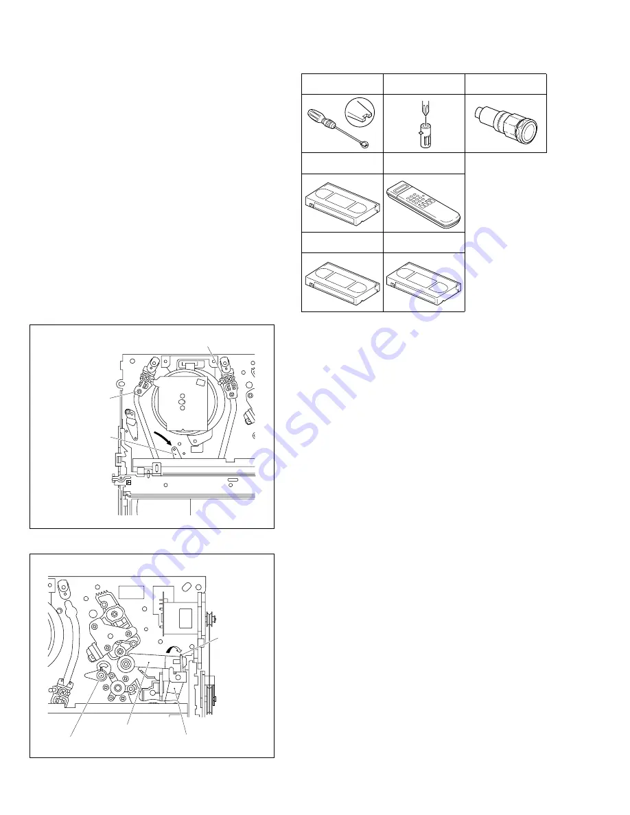
(2) While keeping the tension arm assembly of the mecha-

nism assembly free from tension, pull the tape on the pole
base assembly (supply or take-up side) out of the guide
roller. (See Fig.2-1-3c.)

(3) Take the spring of the pinch roller arm assembly off the

hook of the press lever assembly, and detach it from the
tape. (See Fig.2-1-3d.)

(4) In the same way as in the electrical failure instructions in

2.1.3-1(5), remove the top guide.

(5) Raise the cassette tape cover. By keeping it in that posi-

tion, draw out the cassette tape case from the cassette
holder and take out the tape.

(6) By hanging the pinch roller arm assembly spring back

on the hook, take up the slack of the tape into the cas-
sette.

Fig. 2-1-3d

Fig. 2-1-3c

Pole base assembly (take-up side)

Pole base assembly

 (supply side)

Tension arm assembly

Guide pole guard

Pinch roller arm assembly

Press lever assembly

Take the spring 
off the hook, and 
detach it from the 
tape.

2.1.4 Jigs and tools required for adjustment

Roller driver

PTU94002

A/C head positioning tool

PTU94010

Back tension cassette gauge

PUJ48076-2

Jig RCU

PTU94023B

Torque gauge

PUJ48075-2

Alignment tape

(SP, stairstep, PAL)

MHPE

Alignment tape

(LP, stairstep, PAL)

MHPE-L

Содержание HR-S6850MS

Страница 1: ...L EP 220 lignes VHS PAL EP 240 lignes VHS SECAM VN LD Gamme de fréquence 70 Hz à 10 000 Hz Audio normal 20 Hz à 20 000 Hz Audio Hi Fi Entrée sortie Connecteurs péritélévision à 21 broches ENTREE SORTIE x 1 ENTREE DECODEUR x 1 Connecteurs RCA ENTREE VIDEO x 1 ENTREE AUDIO x 1 SORTIE AUDIO x 1 Connecteurs S Vidéo ENTREE x 1 SORTIE x 1 SYNTONISEUR Système de syntonisation Syntoniseur à synthèse de fr...

Страница 2: ...Clearing the EMG history 1 5 1 8 3 EMG content description 1 6 1 8 4 EMG detail information 1 1 7 1 8 5 EMG detail information 2 1 8 2 MECHANISM ADJUSTMENT 2 1 Before starting repair and adjustment 2 1 2 1 1 Precautions 2 1 2 1 2 Checking for proper mechanical operations 2 1 2 1 3 Manually removing the cassette tape 2 1 2 1 4 Jigs and tools required for adjustment 2 2 2 1 5 Maintenance and inspect...

Страница 3: ...e specified for compli ance with recognized codes pertaining to X ray emission Consequently when servicing these products replace the cath ode ray tubes and other parts with only the specified parts Under no circumstances attempt to modify these circuits Unauthorized modification can increase the high voltage value and cause X ray emission from the cathode ray tube 12 Crimp type wire connector In ...

Страница 4: ... between terminals and surrounding metallic parts See table 1 below 4 Leakage current test Confirm specified or lower leakage current between earth ground power cord plug prongs and externally exposed accessible parts RF terminals antenna terminals video and audio input and output terminals microphone jacks earphone jacks etc Measuring Method Power ON Insert load Z between earth ground power cord ...

Страница 5: ...bers are also used as the identification location No of parts Figures 2 Part name to be removed or installed 3 Fig No showing procedure or part location 4 Identification of part to be removed unhooked unlocked released unplugged unclamped or unsoldered P Spring W Washer S Screw L Locking tab SD Solder CN WR Remove the wire WR from the connector CN Note 2a When reattaching the Front panel assembly ...

Страница 6: ... S1a S1c S1c Bracket 1 Top cover 1 S1b Procedures for Lowering the Cassette holder assembly S3b 3 Drum assembly CN1 CON1 WR3a Note 2c L3a L3b P3 Roller arm assy Inertia plate L3c WR3b Note 2c Cleaner assy Not used Not used S3a S3c Drum shield S3d Note When installing the Drum assembly secure the screws S3a to S3c in the order of a b c Turn the loading motor pulley in the direction as indicated by ...

Страница 7: ...acer Note 4a CN2001 A C head base WR4a Note When installing the Mechanism assembly secure the screws S4a to S4b in the order of a b L4 Spacer Note 4a WR4a Note 2c S3002 S cassette switch Note 4a Fig D4 Fig D6 Fig D5 5 Main board assembly L5a S5a S5c S5c WR5a S5b S P Converter board assy CN1601 L6b 6 Bottom cover L6b L6b L6a Note 6a ...

Страница 8: ...the front slide the holder in the same direction as the cassette insertion di rection For the positions of lock levers A B refer to the Procedures for lowering the Cassette holder assem bly of 1 3 Disassembly assembly method 5 The cassette holder lowers and when the loading has completed the mechanism enters the desired mode 1 6 Jig RCU mode This unit uses the following two modes for receiving rem...

Страница 9: ... 2 Transmit the code 36 from the Jig RCU 3 Reset the EMG display Example 1 E 01 03 Previous EMG Latest EMG No EMG record Example 2 E 1 8 1 Displaying the EMG information 1 Transmit the code 59 from the Jig RCU The FDP shows the EMG content in the form of E INITIAL MODE DATA CODE CUSTOM CODE 43 A CODE Data transmitting method Depress the 3 button after the data code is set Jig RCU Notes The EMG det...

Страница 10: ...housing load increases during ejection the loading motor is stopped because of lack of headroom in its drive torque Housing load increasing factors Temperature environment low tempera ture etc mechanism wear or failure 3 The sensor switch for detecting the end of ejection are not functioning normally 4 The loading motor drive voltage is lower than specified or power is not sup plied to the motor M...

Страница 11: ...EV SEARCH x1 speed reverse playback using JOG CD AUDIO DUB PAUSE EF INSERT REC VIDEO AUDIO PAUSE F0 Mechanism being initialized F1 POWER OFF as a result of EMG F2 Cassette being inserted F3 Cassette being ejected F4 Transition from STOP with pinch roller pressure on to STOP with pinch roller pressure off F5 Transition from STOP with pinch roller pressure on to PLAY F6 Transition from STOP with pin...

Страница 12: ...assette thick tape TC 10 09 15 C cassette thick tape TC 20P 0A 0B Small reel thick tape T 20 0A 16 C cassette thin tape TC 30 0A 16 C cassette thin tape TC 40 0D 0F Small reel thick tape T 40 11 14 Small reel thick tape T 60 15 18 Small reel thick tape T 80 DF 160 17 1A Small reel thick tape T 90 DF 180 19 1D Small reel thick tape T 100 1D 21 Small reel thick tape T 120 DF 240 1E 1F Small reel thi...

Страница 13: ...ch is loaded be cause of any electrical failure manually remove it by taking the following steps 1 Unplug the power cord plug from the power outlet 2 Refer to the disassembly procedure and perform the dis assembly of the major parts before removing the drum assembly 3 Unload the pole base assembly by manually turning the loading motor of the mechanism assembly toward the front In doing so hold the...

Страница 14: ... 1 3d 4 In the same way as in the electrical failure instructions in 2 1 3 1 5 remove the top guide 5 Raise the cassette tape cover By keeping it in that posi tion draw out the cassette tape case from the cassette holder and take out the tape 6 By hanging the pinch roller arm assembly spring back on the hook take up the slack of the tape into the cas sette Fig 2 1 3d Fig 2 1 3c Pole base assembly ...

Страница 15: ...d Press lever assembly Lid guide Guide arm assembly Reel disk take up side Sub brake assembly take up side Main brake assembly take up side Idler arm assembly Idler lever Main brake assembly supply side Reel disk supply side Rec safety lever Tension brake assembly Adjust pin Tension arm assembly Pole base assembly supply side Full erase head Pole base assembly take up side T1 T26 T25 T24 T23 T22 T...

Страница 16: ...y as this will cause damage to the video head 2 To clean the parts of the tape transport system other than the upper drum use a piece of closely woven cloth or a cotton swab soaked with alcohol 3 After cleaning make sure that the cleaned parts are com pletely dry before using the video tape 3 Lubrication With no need for periodical lubrication you have only to lu bricate new parts after replacemen...

Страница 17: ...ry encoder B 1 2 2 11 Clutch unit B 1 2 2 12 Change lever assembly B 3 2 2 12 Direct gear B 4 2 2 12 Coupling gear B 5 2 2 12 Clutch gear B 6 2 2 13 Link lever B 1 2 2 14 Cassette gear B 2 2 2 14 Control cam B 2 2 2 14 Worm gear B 1 Lid guide T B 5 2 2 15Control bracket1 B 1 2 2 15Control plate B 6 2 2 16Loading arm gear supply side B 7 2 2 16Loadingarmgear take upside B 8 2 2 16Loading arm gear s...

Страница 18: ...ration in response to phases of the rotary encoder internal switch positions the mechanism may not operate properly unless such parts as the rotary encoder control plate loading arm gear control cam cassette gear limit gear relay gear and drive gear are installed in their correct posi tions Especially this model is not provided with any cassette hous ing assembly so that cassette loading and unloa...

Страница 19: ...y into the groove See Fig 2 2 3g 4 While swinging the lock lever R of the cassette holder assembly toward the front put the legs A and B into the rail See Fig 2 2 3g 5 Drop the three legs on the left side of the cassette holder assembly into the groove at one time See Fig 2 2 3h 6 Slide the whole cassette holder assembly toward the front to bring it to the eject end position 7 Install the limit ge...

Страница 20: ...replacing only the A C head remove the three screws B while controlling the compression spring Fig 2 2 6a Fig 2 2 6c Fig 2 2 4a 2 2 5 Guide arm assembly and press lever assembly 1 How to remove 1 Remove the spring and expand the lug of the lid guide in the arrow indicated direction Then remove the guide arm assembly by pulling it up 2 Remove the press lever assembly by pulling it up See Fig 2 2 5a...

Страница 21: ...mbly are correctly in stalled as indicated in Fig 2 2 8b 3 Making sure that the connector for the capstan motor is correctly mounted and securely tighten the three screws A Note When the capstan motor has been replaced with a new one perform recording in the EP or LP mode for at least 2 minutes at normal temperatures immediately be fore starting the FF REW or SEARCH operations Ag ing Spacer Spacer...

Страница 22: ...the rotary encoder guide in the arrow indicated direction and remove the change lever assembly 2 Remove the slit washer retaining the direct gear and re move the latter Take care so as not to lose the washer and spring See Fig 2 2 12a 2 2 10 Rotary encoder 1 How to remove 1 Remove the screw A and remove the rotary encoder by pulling it up See Fig 2 2 10a Fig 2 2 10a Rotary encoder Front side Screw...

Страница 23: ...t of the rotary encoder guide Mark E Fig 2 2 13c Worm gear Control cam Main deck guide hole Control cam guide hole Cassette gear 2 2 14 Cassette gear control cam and worm gear 1 How to remove 1 Remove the control cam by lifting it 2 Open the two lugs of the cassette gear outward and pull the latter off 3 Remove the belt wound around the worm gear and the loading motor 4 Open the lug of the lid gui...

Страница 24: ...embly shaft Section D Section D Section A Hole A 3 Install the control plate so that the section A of the load ing arm gear shaft fits into the hole A of the control plate the section B of the control plate guide into the hole B and the control plate comes under the section C of the rotary encoder guide and the section D of the loading arm gear shaft while press fit the pole base assmebly sup ply ...

Страница 25: ...e main deck 3 Remove the lugs B and C of the sub brake assembly take up side from the main deck and remove the sub brake assembly take up side Fig 2 2 19a Spring Sub brake assembly take up side Lug B Lug A Lug C Fig 2 2 20a Lug D Lug C Spring Lug E Lug A Lug B Main brake assembly take up side Reel disk take up side Main brake assembly supply side Notch 2 2 20 Main brake assembly take up side reel ...

Страница 26: ...2 Remove the reel disk supply side by loosening in the arrow indicated direction the main brake assembly sup ply side 3 Remove the tension spring on the back of the main deck Then release the lug of the tension arm bearing in the arrow indicated direction and draw out the tension arm assembly See Fig 2 2 21a Fig 2 2 21a Lugs Tension brake assembly Lug of the tension arm bearing Reel disk supply si...

Страница 27: ...stall a new washer and upper drum assembly on the drum shaft See Fig 2 2 25a 3 Install the cap to the upper drum assembly 4 Position the collar assembly as indicated in Fig 2 2 25c while controlling its up down movement 5 Secure the collar assembly in position with a hexagonal wrench while pressing its top with the fingers 6 After installation gently turn the upper drum assembly with your hand to ...

Страница 28: ...ed See Fig 2 3 1a 5 Reduce the V PB FM waveform by the tracking opera tion If a drop in level is found on the left side turn the guide roller of the pole base assembly supply side with the roller driver to make the V PB FM waveform linear If a drop in level is on the right side likewise turn the guide roller of the pole base assembly take up side with the roller driver to make it linear See Fig 2 ...

Страница 29: ...scope Measuring point D TP106 PB FM External trigger E TP111 D FF Adjustment part F A C head base Mechanism assembly Specified value G Maximum V PB FM waveform Adjustment tool H A C head positioning tool PTU94010 1 Play back the alignment tape A1 2 Apply the external trigger signal to D FF E to observe the V PB FM waveform at the measuring point D 3 Set the VCR to the manual tracking mode 4 Loosen...

Страница 30: ...point D TP106 PB FM External trigger E TP111 D FF Adjustment part F Jig RCU Code 50 Specified value G STOP mode Maximum V PB FM waveform Adjustment tool H Jig RCU PTU94023B 2 3 5 Tension pole position 1 Play back the back tension cassette gauge A 2 Check that the indicated value on the left side gauge is within the specified value G 3 If the indicated value is not within the specified value G perf...

Страница 31: ...304 2 320 4 335 IN FF REW OUT PLAY Direct gear Change lever 2 ON HALF REV HALF FF REW OFF Tension arm ON CONTACT OFF Main brake S ON CONTACT OFF Main brake T ON OFF Sub brake S ON OFF Sub brake T ON OFF OFF ON Capstan brake ON OFF Rec safety switch Operation mode ON PLAY ON REV CONTACT OFF C INS Pinch roller SUPPLY CENTER TAKE UP Idler position READY RESET Take up lever ON OFF Guide arm Timer REC ...

Страница 32: ...by the EVR system The main unit have EEPROMs for storing the EVR adjustment data and user setups Notes In the EVR adjustment mode the value is varied with the channel buttons The adjusted data is stored when the setting mode changes from PB to STOP when the tape speed is changed etc Take care to identify the current mode of each adjustment item when making an adjustment When changing the address s...

Страница 33: ...mode by transmitting the code F from the Jig RCU When the VCR enters the stop mode the adjustment is completed 6 If the VCR enters the eject mode repeat steps 1 to 5 again 7 Play back the alignment tape A2 again confirm that the switching point is the specified value G Fig 3 3 1a D A level 1 Insert the cassette tape A3 to enter the mode B 2 Observe the VIDEO OUT waveform at the measuring point D 3...

Страница 34: ...firmation and re adjustment of the item 3 4 1 Fig 3 3 3b REC color colour level V rate Specified value G 7 Set the VCR to the EVR mode by transmitting the code F1 from the Jig RCU 8 Set the EVR address to F2 by transmitting the code F3 from the Jig RCU 9 Transmit the code F4 from the Jig RCU to adjust so that the higher level channel becomes the specified value G of the note B level as shown in Fi...

Страница 35: ... marker D2 Specified value G 5 MHz V rate Scale 4 4 div Fig 3 3 4a Video EQ Frequency Response 4 If the A PB FM level is not within the specified value G1 perform the adjustment in a following procedure 5 Set the VCR to the EVR mode by transmitting the code F1 from the Jig RCU 6 Set the EVR address to F2 by transmitting the code F3 from the Jig RCU 7 Transmit the code F4 from the Jig RCU to adjust...

Страница 36: ...oscope Measuring point D1 CN1601 Pin 7 D2 CN1601 Pin 3 Adjustment part F VR1603 Specified value G T 5 6 0 1 µsec 3 6 1 Colour difference level 1 Observe the C converted colour waveform at the meas uring point D 2 Adjust the adjustment part F1 so that the higher level of the Yellow and Blue of the C waveform becomes the specified value G1 3 Adjust the adjustment part F2 so that the higher level of ...

Страница 37: ...PB Alignment tape colour bar SP mode normal VHS mode 2 Audio circuits REC 1KHz 8 dBs sine wave signal in SP mode normal VHS mode PB REC then playback it 3 Movie Camera circuits Measured using a correctly illuminated gray scale or colour bar test chatrs in the E E mode 4 Indication on schematic diagram Waveform indications on the schematic diagram are as shown below 5 Waveform indications Waveform ...

Страница 38: ... 6 Signal path Symbols The arrows indicate the signal path as follows Playback signal path Playback and recording signal path Recording signal path including E E signal path Capstan servo path Drum servo path Example R Y Y Playback R Y signal path Recording Y signal path 7 Indication of the parts for adjustments The parts for the adjustments are surrounded with the circle as shown below 8 Indicati...

Страница 39: ...AP FG SW5V CAP REV L CAP CTL V M12 17V FULL ERASE GND LOADING MOTOR ROTARY ENCODER LP EP CH2 D FG CN2001 CN2002 CN3001 CN3003 CN3004 CN3002 7 8 09 9 CN7005 JSA NC NC NC 8 NC 3 8 CN7002 CN7003 CN7004 OR 9 8 7 6 5 4 3 2 1 0 3 CN7001 9 8 7 6 5 4 3 2 1 0 3 CN7001 9 8 7 FLY E FLY E FLY E I2C I2C DATA CLK TU A MUTE DEMOD DEMOD R L 28 SW5V MINI FRONT ADV JOG 38 6 5 GND 4 COMP SIF NC GND C FROM DIGI KILLE...

Страница 40: ...2052 Q2054 R2051 R2053 T2051 R2060 R2059 R2058 R2057 CN2001 Q2062 C2061 T2052 Q2061 R2062 R2061 C2062 C2063 C2064 R2064 R2063 CN2002 B2051 FULL_E ON H R2065 C2228 R2228 R2229 R2020 Q2005 C103 C93 L17 MESECAM H R75 R77 L12 L5 R79 R113 K2253 K2252 C2230 C2229 D6 R88 B50 R33 B12 B25 180p 12p 100K 1 8k 47p 47 68µ 0 1 0 1 0 01 0 1 0 01 0 1 0 1 1 3 3 2 2 3 3 12µ 10µ 47 0Ω 0Ω 10 4 7 10µ 0 1 1 27k 1 8K 68...

Страница 41: ...S CLK S DATA_FRSYS R204 R203 R202 1 1 5k 0 47 220 0Ω 1 1k 2 2k 10µ 1µ 0Ω 100 470 5 6K 100 22µ 100 100 0 01 220 10K 56p 22µ 0 22 0 22 1 8k 4 7 0 1 100p 100p 33p 33p 10k 10 50 2SC4081 QRS OPEN OPEN OPEN 2SA1576A QR SHORT SHORT SHORT VSS1 XTAL_IN MUTE CHABLK LN21 OSC_IN OSC_OUT SYNC_DET CS SCLK SDATA VDD2 CR_OUT VCO_IN1 VSS3 VDD3 VCO_R NC CVOUT VSS2 CV_IN CVCR VDD1 SYNC_IN SEP_C SEP_OUT I2C_DATA CDLR...

Страница 42: ...13 C317 R312 R315 R309 R304 R316 C308 C321 IC301 0 47 1 820 100µ 0 0 47 1 1 1 39p 10µ 47 24k 120k 0 0068 0 0068 0 1 0 01 0 01 0 01 6 8µ 27k 150p 47k 2 2k 2 2k 27k 27k 150p 0 001 0 022 0 01 0 01 27µ 4 7k 22k 22k 680p 2 7k 560k 0Ω 6 8k 120k 0 01 300p OPEN OPEN OPEN OPEN OPEN SHORT 6 3 2SA1576A QR 2SB1218A QR 2PA1576 R 0 5 OPEN OPEN OPEN OPEN DTA144WUA UN511E RN2309 PDTA144WU OPEN 2 LA7358 FILT 0 3 M...

Страница 43: ... 0 1 0 1 1k 1k 1k 1k 1k 1k 6 8k 1k 5 6k 1k 1k 1k 1k 0 470 1k 1k 1k 0 0 10k 30p 0 1 4 7k 1k 47 10k 1k 1k 0 1k 1k 560 4 7k 1k 100 1k 1k 0 470 2 2k 4 7k 10k 1k 0 0 0 0 1k 0 0 0 0 2 2k 2 2k 0 1 1k 4 7k 0 01 1k 0 0 100p 0 1k 1k 0 1k 1 5k 1k 4 7k 0 100p 22 0 0 0 470 470 470 1k 1k 1k 0 1 0 1 10k 2 2k 4 7k 10k 10 0 1 18k 18k 12p 180 330k 470k 180 180 10k 27k 27k 18p 1 10k 10K 4 7k 10 0 1 4 7k 47 47 0 0 0 ...

Страница 44: ...20 R5321 Q5308 B5301 47k 220 100 47k 270p 10 100µ 0 068 0 033 100 100 220 0 0047 100 68 0 39 330 1 68k 10k 0 001 33p 10 1200 680 220 0 01 4 7 470 47 33µ 33µ 0 0022 1k 220 47 100 T2AL 47 180 4 7k 2 2k 2 2k 1k 220 220 0 1 220k 470 10k 4 7k 1k 220 0 22 560 3 3k 1 2k 3 3k 2 2k 4 7k 0 018 680 560 1 2k 1k 2 2k 1k 27k 27k 2SD1450 ST 2SD1302 ST 1 4W FR S1WB A 60 4102 S1WB A 60 S1WB A 60F4072X DTA114EUA UN...

Страница 45: ...N6701 C6056 R6020 R6021 B6510 R6050 R6031 C6037 L6003 Q6032 TU_A_MUTE H C6006 C6005 D6002 C6027 C6028 R6052 R6051 C6053 C6052 C6016 C6020 GND Q6030 Q6031 R6030 R6032 C6021 R6033 TU_AUDIO RF_AUDIO GND TU_VIDEO RF_VIDEO C6023 C6032 DEMOD R DEMOD L SW2 SW1 C6013 C6012 C6008 C6007 L6001 22p 22p 1k 1k 100 270 10 0 01 10 220p 220p 100p 100p 1k 0 0 047 0 01 BB AL5V TU 30V NC AS SCL SDA NC MB SW5V LOCK TU...

Страница 46: ...2 MTZJ9 1B UZ9 1BSB OPEN OPEN F F NP NC 6G 5G 4G 3G 2G 1G P16 P15 P14 P13 P12 NC NC NC NC NC P11 P10 P9 P8 P7 P6 P5 P4 P3 P2 P1 NC NP F F OPEN OPEN JSA OPEN OPEN OPEN FRONT Y SW DISPLAY MAIN 0 3 TEST R7017 R7018 S7014 S7015 D7008 D7009 LED for S7002 for S7016 SYMBOL PHILIPS RCU JVC TO R7010 C7004 D7002 IC7003 SHORT GP1U291Q PNA4652MOOYC PIC 28143LJ GP1U290Q PNA4655MOOYC PIC 28142LJ AJ FDP AJ Adv J...

Страница 47: ...0 4 7k 10µ SCR H CH 12 SW12V LI_5V GND I2C_CLK2 I2C_DATA2 P50_I O 3 58NTSC H P ON_P TU_VIDEO Fsc Y_FROM_DIGI GND GND Y V_TO_DIGI C_TO_DIGI C_FROM_DIGI GND GND DEC OUT R DEC OUT L GND A IN1 L A IN1 R A OUT L A OUT R A IN2 L A IN2 R SAT_CTL_OUT R PAUSE PB_COLOR FRONT_Y_IN ADJ SECAM_PB_COLOR MAIN_ALC_DET Y_TO_SUB P MUTE L FRONT_V_IN V_TO_OSD CHARA_DATA V_FROM_OSD GND GND I2C_CLK I2C_DATA GND V_FROM_A...

Страница 48: ...42 C1241 B1204 R1224 C1243 C1244 D1203 D1202 R1223 C1246 C1229 C1245 C1247 R1229 C1249 R1228 Q1206 R1227 C1248 R1226 R1225 R1230 R1231 R1233 R1232 C1250 1 300 0 1 0 1 100µ 100µ 47 100µ 100µ 47 0 01 5 6k 0 1 12k 0 001 1 18 0 1 0 1 39k 10k 10k 100 6 8µ 27p 82p 330 1k 100 6 8µ 82p 27p 330 1k 220 220 1k 47 4 7 560 1µ 33p 100p 47 100µ 120 100 47 0 1 0 1 0 1 0 1 0 1 0 1 15µ 18p 56p 470 0Ω 560 0 01 4 7 4...

Страница 49: ...B1409 C1466 C1467 C1469 C1468 Q1406 R1405 Q1404 IC1401 R1454 1 470 10 1 8k 100k 470 6 8µ 0 1 39p 0 01 33k 39k 10µ 330 33p 68p 220 2 2k 2 7k 1µ 1 5k 820 0 1 0 01 100 6 8k 0Ω 680 47 0 1 0 1 0 1 0 1 6 8µ 68p 0 1 33p 560 0 1 4 7 680 27k 0 1 0 1 0 1 820 1 3 9k 0 1 0 1 0 1 15k 22k 6 8k 10k 0 1 0 1 0 1 0 1 1 8k 2 2k 1 5k 33µ 22p 39p 6p 51 0 1 0 01 33 27k 120 10K 0 1 0 1 680 1k 1k 470 470 1k 1k 1k 0 1 6 8...

Страница 50: ... L I2C_CLK I2C_DATA GND REC_COLOR GND GND V_FROM_AV Y_TO_AV SW5V SW5V SW5V FROM_PS_Y GND GND GND TO_PS_Y FROM_PS_C TO_PS_C SW12V SW12V 50 50 2 CH VC2076DP PB_COLOR FRONT_Y_IN ADJ SECAM_PB_COLOR MAIN_ALC_DET Y_TO_SUB P MUTE L FRONT_V_IN V_TO_OSD CHARA_DATA V_FROM_OSD GND GND 16 6 3 50 50 50 50 0 5 0 5 0 5 0 5 0 5 SHORT 0 5 50 50 2 CH 2 CH CH CH 2 CH 2 CH 2 CH 6 3 2 CH OPEN OPEN 6 3 0 6 TERMINAL S S...

Страница 51: ...3 R921 R922 R919 R920 10µH 100 75 75 100 470 510 100 75 0 100 75 0 0 01 100 75 15µ 0 10µH 10µH 10µH 100 100 100 100 4 7µ 4 7µ 4 7µ 0Ω 0 022 15µ 75 75 4 7µ 47 5 6k 3 3k 330p 330p 470p 5 6k 1µ 470p 330p 330p 33p 470p 470p 4 7µ 4 7µ 4 7µ 4 7µ 75 10 100 470p 47 47 1K 0Ω 0Ω 75 220 100 0 001 10 0 022 0 022 0 022 75 75 330p 330p 1µ 470p 330p 330p 100 0 22µ 470p 1k 75 100 100 10k 0 01 4 7k 0 1k 560 6 8k 2...

Страница 52: ...47 47 47 47 47 47 47 47 FE 600 FE 600 FE 600 FE 600 FE 600 FE 600 FE 600 FE 600 8p 8p 8p 7p 7p 7p 7p 7p 1p 1p 1p 3p 3p 3p 3p 3p C6708 C6709 X TAL DAC OUT R6713 R6715 C6714 C6716 0 0068 0 0068 0 0068 0 0068 0 0022 0 0022 0 0022 0 0022 VREF C6722 C6723 0 01 0 01 0 01 0 01 0 01 0 01 0 01 0 001 IC6701 C6719 C6706 K6701 K6702 C6707 X6701 C6709 C6708 K6703 K6704 R6709 R6708 C6710 C6711 K6705 R6710 C6721...

Страница 53: ...1 47 0 01 47 1 1 0 22 0 01 47 0 22 12p 180k 100k 560 3 3k 1 2k 0 22 1000p 2200p 10k 470k 1 100p 130k 470k 330 1 0 01 100k 1k 10µ 1 5k 1 5k 0 01 22k 560 3 3k 47 47 0 01 10k 33k 27k 470 470 680 1k 560 2 2k 0 01 10µ 47 3 3k 0 01 0 01 470 10k 10k 1 2k 0 01 1p 100 680 330 470 1 2k 1k 1k 1k 2 7k 10µ 0 01 47k 56k 680 1 2k 680 2 2k 330 22 47 100 680 330 470 1 2k 1k B Y n c n c CVBS fref TEST GND n c SSC n...

Страница 54: ...0 31 E B 16 AUDIO IN R AUDIO IN L VIDEO IN REC S 8 4 SENSOR END D FF CTL P PB FM A PB FM 2 1 4 8 7 4 5 1 9 1 TAKE UP 4 84 85 56 57 29 1 112 28 E E B 8 1 4 2 S CASS 8 1 9 2 21 6 2 5 1 5 1 9 30 A 5 1 1 BROWN BLUE 91 S ET SAT SAT PLAY STOP EJECT PAUSE REC E PROG 5 4 1 15 14 28 6 7 1 2 1 6 4 120 1 3 4 1 2 3 1 2 1 10 1 10 1 12 6 4 30 3 8 5 4 1 15 B E V2 FF REW 60 DI7001 CN901 CN902 CN903 R4006 D3001 PC...

Страница 55: ...9 B C 10D R3020 B C 10D R3021 B C 10D R3022 B C 10D R3025 B C 11D R3026 B C 11D R3027 B C 9C R3029 B C 11D R3030 B C 11D R3031 B C 11D R3032 B C 11D R3033 B C 11D R3034 B C 9C R3035 B C 9C R3036 B C 9C R3038 B C 12D R3039 B C 12D R3040 B C 12D R3041 B C 12D R3042 B C 14C R3044 B C 15D R3046 B C 13D R3047 B C 12E R3048 B C 14D R3049 B C 12E R3050 B C 12E R3051 B C 12E R3052 B C 13E R3053 B C 12E R3...

Страница 56: ... B C 12B R535 B C 13B R536 B C 13B R901 B C 8D R902 B C 7C R903 A D 7D R904 B C 4D R905 B C 4D R906 A D 4C R907 A D 4C R908 B C 7B R909 B C 7B R910 B C 7A R911 B C 7A R912 B C 4B R913 B C 4B R914 A D 5A R915 A D 6A R916 B C 7C R917 B C 3B R918 B C 3B R919 A D 11B R920 A D 11B R921 A D 11E R922 A D 11D R923 B C 11D R924 B C 10C R925 B C 9D R926 B C 9C R927 B C 2D R928 A D 2D R929 B C 11E R930 B C 1...

Страница 57: ...NT4 P01 SCR 1 12 2 3 5 4 6 8 7 9 10 11 13 14 16 15 17 19 18 20 21 22 23 24 25 26 27 28 S0 S1 S2 S3 S4 S5 S6 S7 S8 S9 S10 S11 S12 S13 S14 S15 S16 S17 S18 S19 COM0 COM1 COM2 COM3 P03 SI SB1 P02 SO SB0 46 4 8 20 28 44 35 7 12 16 31 36 3 11 24 32 43 33 6 18 19 29 42 39 2 10 23 27 45 34 13 14 15 30 41 38 5 17 22 26 40 37 1 9 21 25 p70 p71 p63 p62 p61 p60 p40 p41 p42 p43 p50 p51 p52 p53 X1 1 2 3 C3 C2 X...

Страница 58: ... 0 68 Vp p 10 mV 20 µsec DIV WF6 IC1 105 REC 1 8 Vp p 0 1 V 1 msec DIV WF2 IC1 30 PAL PB 0 68 Vp p 20 mV 20 µsec DIV WF3 IC1 1 PB 0 3 Vp p 20 mV 5 msec DIV WF4 TP106 PB FM PB 0 5 Vp p 20 mV 5 msec DIV WF5 TP111 D FF REC PB 3 4 Vp p 0 1 V 10 msec DIV WF1 IC1 27 PB 2 1 Vp p 50 mV 20 µsec DIV VIDEO WF7 IC1 14 PB 0 5 Vp p 20 mV 20 µsec DIV WF8 IC1 13 REC PB 0 5 Vp p 20 mV 20 µsec DIV WF9 IC1 11 REC PB...

Страница 59: ...4 0 0 5 2 5 2 3 6 0 0 7 3 5 2 4 8 0 0 9 2 8 2 8 10 4 9 4 9 CN902 1 2 8 2 8 2 0 0 3 0 0 4 2 4 2 1 5 1 3 2 3 6 4 9 4 9 7 0 0 8 0 0 9 2 3 2 3 10 0 0 11 0 0 12 2 4 2 1 CN903 1 4 7 4 7 2 0 0 3 0 0 4 0 0 5 0 8 0 8 6 10 1 10 1 7 10 1 10 1 8 4 5 4 5 9 4 5 4 5 10 0 0 CN904 1 0 0 2 4 9 4 9 3 0 0 4 0 2 0 2 5 0 0 2 6 0 0 7 0 0 8 0 0 9 0 0 10 0 0 11 0 0 CN905 1 2 4 2 4 2 0 0 3 2 8 2 8 4 0 0 5 3 3 3 3 6 0 0 7 2...

Страница 60: ...SIGNAL FOR TAKE UP REEL ROTATION TAPE REMAIN 56 JSA IN INPUT FOR THE JOG SHUTTLE PIN NO LABEL IN OUT FUNCTION PIN NO LABEL IN OUT FUNCTION SYSCON IC3001 CHANGES IN ATS IC OUTPUT AS CAUSED BY CHANGES IN RECEIVER SENSITIVITY WHEN THE SAME CHANNEL IS RECEIVED MORE THAN ONCE ARE INPUT 57 JSB IN INPUT FOR THE JOG SHUTTLE 58 REC_SAFETY IN REC SAFETY SWITCH DETECT SW ON L 59 SW1 OUT TUNER SYSTEM MODE H 6...

Страница 61: ...TO VIDEO AUDIO N REC_ST H N REC_ H H REC_ST H I2C_CLK_A V I2C_DATA_A V A FF A MUTE H TO Vcc X3001 32KHz TIMER X3002 CLOCK MAIN 10MHz TP3905 SP_FG LMC3 LSB LSC LSA 25 27 26 LMC2 LMC1 36 37 35 TU_FG 55 START_SENSOR END_SENSOR 14 66 15 S CASS H OSD_CS 47 46 DFG 54 DPG DRUMPWM 107 108 102 CAP_REV L 101 CFG CAPPWM 8 28 REC_SAFETY S DATA_TOSYS S DATA_FRSYS S CLK OSC1 IN 58 51 52 53 67 X2 OSC2 OUT X1 69 ...

Страница 62: ...YOUT IIC_DATA IIC_CLK PB COMB REC REC 44 41 35 34 SEP MIX 0 5 BUF Q1202 DIGITAL 2D CN1201 19 V_TO_OSD CHARA_DATA Y_TO_AV V_FROM_AV REC_COLOR 16 29 30 15 14 Y_FROM_DIGI C_FROM_DIGI PB_COLOR MAIN_ALC_DET P MUTE L Y_TO_SUB FRONT_V_IN 25 28 27 26 24 20 21 I2C_DATA I2C_CLK Fsc C_TO_DIGI Y V_TO_DIGI 17 18 13 12 I2C_DATA_A V I2C_CLK_A V C_FROM_DIGI Y_FROM_DIGI V Y_TO_DIGI C_TO_DIGI Fsc 10 8 9 6 3 4 5 USE...

Страница 63: ...XTAL_ SDATA 2 IN 11 CS CHABLK 10 9 4 BUF Q903 SCREEN Y IC201 2Fsc Y 3 Q904 BUF 4 2 C 1 S CLK OSD_CS REAR S OUT J904 HEAD_SEL VIDEO_ENV I2C_DATA2 SYNC_DET H NORM MESEC S SYSCON R P Adj MOD YCA Clamp 6 12 13 R P R P 14 P R FBC ALC DO REC SQPB EQ SQPB SQPB ET R Y LPF P ET LPF ET De Emph Main DeMOD LPF Sub 7 SW Q17 Main Emph Carrier C D C W Offset S DET fo Dev FM REC Filter TRAP HPF Det Killer Emph N ...

Страница 64: ... EP LP ON ON REC R P AMP PRE ON SP TRANS FILTER 119 117 118 FILTER 116 115 Q2061 T2052 4 6 OSC A C 1 2 1 4 3 6 7 4 5 CN2001 CN1 HEAD 2 ERASE FULL 2 1 HEAD A ERASE REC PB F ERASE A MUTE AMP R CH EVR L CH L CH REDUCTION NOISE NA PB R CH EVR REDUCTION NOISE R CH HIFI CH1 FM CH2 COMMON MON PRE REC NOR DET PROCESSOR SIGNAL AUDIO REC PB DATA ENV LOGIC DET CLK POWER Q2251 Q2252 97 96 Q2062 Q2063 A PB FM ...

Страница 65: ...TE CONTROLLER A B C 306A LP40254 006A COVER BATTERY D LP40610 002A COVER BATTERY A B C REF No PART No PART NAME DESCRIPTION REF No PART No PART NAME DESCRIPTION 307 BATTERY X2 R6 TYPE 308 QPC02202230P POLY BAG 310 LPT0493 001A INST BOOK FR A LPT0494 001A INST BOOK FR B C LPT0495 001A INST BOOK FR D 311 QPC02503530P POLY BAG 312 PEAC0300 02 RF CABLE 313 QAL0095 005 LED CABLE ASSY Satellite Controll...

Страница 66: ...F F MAIN BOARD ASSY 03 TERMINAL BOARD ASSY 06 A H H E B MECHANISM ASSY M4 522 522 OT1 Incl 03 524 514 513 A 508 509 507 507 506 WR1 510 510 505 505F 505E S JACK BOARD ASSY 36 WR4 534 G 501A 501B 529 501 D 533 ADV JOG BOARD ASSY 38 MODEL B C D C 3D DIGITAL 2M BOARD ASSY 05 MODEL D 2D DIGITAL BOARD ASSY 05 MODEL A B C DEMOD BOARD ASSY 14 P 521 520 520A 519 G J F 533 ADV JOG BOARD ASSY 38 MODEL A 532...

Страница 67: ...3 LP30312 001B BRACKET CHASSIS 514 QYTDSF3010Z SCREW X2 515 LP40700 001A SPECIAL SCREW MECHA 516 QYTDSF3010Z SCREW X2 MECHA 517 QMP4A10 170 POWER CORD 519 LP40407 001A KNOB ASSY 520 LP40370 001E ROLLER ARM ASSY 520A PDM4311A 1 ROLLER ASS 521 PQ45160 INERTIA PLATE 522 LP40226 001A PC SUPPORT X2 524 LP40253 001B STOPPER 525 PQ40413 SPECIAL SCREW MECHA 529 LP31019 001C KNOB ASSY FRONT 530 QYTDSF3010Z...

Страница 68: ... 139 130 137 143 138 139 140 129 127 44 43 42 123 AA AA AA AA AA BB AA AA AA AA AA AA AA AA AA AA AA AA BB AA AA AA AA BB 105 120 75 74 121 72 132 76 73 142 88 104 89 135 134 78 107 101 40 106 49 57 54 59 61 62 85 91 1 111 60 83 82 52 58 55 39 53 51 1 112 113 151 116 115 117 118 114 119 66 63 68 67 65 64 70 23 25 24 18 19 20 16 27 71 87 22 99 96 100 31 80 81 34 37 35 103 32 102 36 38 108 109 90 92...

Страница 69: ...N SPRING 74 LP40109 003D TENSION BRAKE ASSY 75 PQ46302 1 3 ADJUST PIN 76 LP30232 002A TENSION ARM BEARING 78 LP40532 008B MAIN BRAKE ASSY SUPPLY 80 LP40111 011A MAIN BRAKE ASSY TAKE UP 81 LP30003 026A TENSION SPRING 82 LP40112 001F SUB BRAKE ASSY TAKE UP 83 LP40357 002A TENSION SPRING 84 LP40461 001A CAPSTAN BRAKE ASSY 85 QAR0087 005 CAPSTAN MOTOR 86 QYTDSF2606M SCREW X3 87 LP30005 007A BELT CAPST...

Страница 70: ...6 R X TRANSISTOR Q24 2SB1218A QR X TRANSISTOR or 2PA1576 R X TRANSISTOR or 2SA1576A QR X TRANSISTOR Q25 DTC144WU TRANSISTOR D or PDTC144WU TRANSISTOR D or RN1309 TRANSISTOR D or UN521E TRANSISTOR D Q38 2SD1819A QRS X TRANSISTOR or 2SC4081 QRS X TRANSISTOR or 2PC4081 R X TRANSISTOR Q40 DTC144WU TRANSISTOR A B C or PDTC144WU TRANSISTOR A B C or RN1309 TRANSISTOR A B C or UN521E TRANSISTOR A B C Q41 ...

Страница 71: ... Q5301 2SB1256 TRANSISTOR Q5302 2SD2375 QP TRANSISTOR Q5303 2SD1819A RS X TRANSISTOR or 2PC4081 R X TRANSISTOR or 2SC4081 RS X TRANSISTOR Q5304 2SC3616 ML T TRANSISTOR Q5305 DTA114EU TRANSISTOR or PDTA114EU TRANSISTOR or UN5111 TRANSISTOR or RN2302 TRANSISTOR Q5306 DTC114EU TRANSISTOR or PDTC114EU TRANSISTOR or UN5211 TRANSISTOR or RN1302 TRANSISTOR Q5308 2SA1576A RS X TRANSISTOR Q5311 DTC114TU TR...

Страница 72: ... or 1SS270A DIODE D7004 1SS133 DIODE or 1SS270A DIODE D7005 1SS133 DIODE or 1SS270A DIODE D7006 1SS133 DIODE B C D or 1SS270A DIODE B C D D7008 SLR 325MC T LE DIODE D7009 SLR 325VC T LE DIODE R1 NRVA02D 682X CMF RESISTOR 6 8kØ 1 10W R2 NRVA02D 152X CMF RESISTOR 1 5kØ 1 10W R3 NRSA02J 182X MG RESISTOR 1 8kØ 1 10W R4 NRSA02J 0R0X MG RESISTOR 0Ø 1 10W R5 NRSA02J 0R0X MG RESISTOR 0Ø 1 10W R6 NRSA02J 2...

Страница 73: ...STOR B C D 15kØ 1 10W R2055 NRSA02J 3R3X MG RESISTOR 3 3Ø 1 10W R2056 NRSA02J 820X MG RESISTOR A 82Ø 1 10W NRSA02J 101X MG RESISTOR B C D 100Ø 1 10W R2057 NRSA02J 473X MG RESISTOR 47kØ 1 10W R2058 NRSA02J 183X MG RESISTOR 18kØ 1 10W R2059 NRSA02J 473X MG RESISTOR 47kØ 1 10W R2060 NRSA02J 183X MG RESISTOR 18kØ 1 10W R2061 NRSA02J 273X MG RESISTOR B C D 27kØ 1 10W R2062 NRSA02J 3R3X MG RESISTOR B C ...

Страница 74: ... QRE141J 183Y RESISTOR 18kØ 1 4W R3208 NRSA02J 181X MG RESISTOR 180Ø 1 10W R3209 NRSA02J 273X MG RESISTOR 27kØ 1 10W R3210 NRSA02J 181X MG RESISTOR 180Ø 1 10W R3211 NRSA02J 273X MG RESISTOR 27kØ 1 10W R3212 QRE141J 474Y RESISTOR 470kØ 1 4W R3213 NRSA02J 334X MG RESISTOR 330kØ 1 10W R3214 NRSA02J 103X MG RESISTOR 10kØ 1 10W R3215 NRSA02J 103X MG RESISTOR 10kØ 1 10W R3216 NRSA02J 103X MG RESISTOR 10...

Страница 75: ... NRSA02J 0R0X MG RESISTOR 0Ø 1 10W B12 QUY160 220Y IM BUS WIRE A B C B13 NRSA02J 0R0X MG RESISTOR D 0Ø 1 10W B25 NRSA02J 0R0X MG RESISTOR 0Ø 1 10W B50 QUY153 050Y IM BUS WIRE B52 NRSA02J 0R0X MG RESISTOR A B C 0Ø 1 10W B55 NRSA02J 0R0X MG RESISTOR 0Ø 1 10W B65 NRSA02J 0R0X MG RESISTOR 0Ø 1 10W B203 QUY153 050Y IM BUS WIRE B204 QUY153 050Y IM BUS WIRE B214 QUY160 280Y IM BUS WIRE B302 NRSA02J 0R0X ...

Страница 76: ...2005 QEKJ1HM 475 E CAPACITOR 4 7µF 50V C2006 NCB21EK 123X CAPACITOR 0 012µF 25V C2007 QEKJ1CM 226 E CAPACITOR 22µF 16V C2008 QEKJ1HM 475 E CAPACITOR 4 7µF 50V C2009 NCB21HK 102X CAPACITOR 0 001µF 50V C2010 NCB21HK 152X CAPACITOR 0 0015µF 50V C2011 QEKJ1HM 475 E CAPACITOR 4 7µF 50V C2012 QEKJ1HM 475 E CAPACITOR 4 7µF 50V C2013 NDC21HJ 680X CAPACITOR 68pF 50V C2015 NCB21HK 682X CAPACITOR 0 0068µF 50...

Страница 77: ...PACITOR 0 01µF 50V C5351 QUY153 050Y IM BUS WIRE C6007 QEMU0JM 227 E CAPACITOR 220µF 6 3V C6008 NCB21HK 103X CAPACITOR 0 01µF 50V C6013 NCB21HK 103X CAPACITOR 0 01µF 50V C6023 NRSA02J 0R0X MG RESISTOR 0Ø 1 10W C6037 QEKJ1EM 106 E CAPACITOR 10µF 25V C6501 QEKJ0JM 107 E CAPACITOR 100µF 6 3V C6502 NCB21HK 103X CAPACITOR 0 01µF 50V C7001 QEKJ0JM 476 E CAPACITOR 47µF 6 3V C7003 QEKJ0JM 227 E CAPACITOR ...

Страница 78: ...0X M FUSE T1 0A 50V F5001 QMF51E2 2R0J1 FUSE T2 0A AC250V 2D DIGITAL BOARD ASSEMBLY 05 MODEL A B C PW1 LPA10090 07A 2D DIGITAL BOARD ASSY IC1201 JCP8036 IC Q1201 2SC1317 RS T TRANSISTOR Q1202 2SA1576A QR X TRANSISTOR or 2PA1576 R X TRANSISTOR Q1203 2SA1576A QR X TRANSISTOR or 2PA1576 R X TRANSISTOR Q1204 2SC4081 QRS X TRANSISTOR or 2PC4081 R X TRANSISTOR Q1205 2SC4081 S X TRANSISTOR Q1206 2SC4081 ...

Страница 79: ...UN521E TRANSISTOR Q1417 2SC4081 QRS X TRANSISTOR or 2PC4081 R X TRANSISTOR Q1418 2SA1576A QR X TRANSISTOR or 2PA1576 R X TRANSISTOR Q1419 DTC124TU TRANSISTOR Q1420 2SC4081 QRS X TRANSISTOR or 2PC4081 R X TRANSISTOR D1401 RD4 3ES B3 T2 ZENER DIODE D1402 1SS133 DIODE or 1N4148M DIODE R1401 NRSA02J 181X MG RESISTOR 180Ø 1 10W R1402 NRSA02J 101X MG RESISTOR 100Ø 1 10W R1404 NRSA02J 182X MG RESISTOR 1 ...

Страница 80: ...25V C1453 NCF21EZ 104X CAPACITOR 0 1µF 25V C1454 NCF21EZ 104X CAPACITOR 0 1µF 25V C1455 NCF21EZ 104X CAPACITOR 0 1µF 25V C1463 QEKJ0JM 336 E CAPACITOR 33µF 6 3V C1468 NDC21HJ 101X CAPACITOR 100pF 50V C1470 NDC21HJ 330X CAPACITOR 33pF 50V C1471 NCF21EZ 104X CAPACITOR 0 1µF 25V C1472 NCF21EZ 104X CAPACITOR 0 1µF 25V C1473 NCF21EZ 104X CAPACITOR 0 1µF 25V L1401 QQL29BJ 100Z COIL 10µH L1402 QQL071J 6R...

Страница 81: ... 103X MG RESISTOR 10kØ 1 10W R941 NRSA02J 332X MG RESISTOR 3 3kØ 1 10W R942 NRSA02J 472X MG RESISTOR 4 7kØ 1 10W R943 NRSA02J 0R0X MG RESISTOR 0Ø 1 10W R944 NRSA02J 272X MG RESISTOR 2 7kØ 1 10W R945 NRSA02J 102X MG RESISTOR 1kØ 1 10W R946 NRSA02J 561X MG RESISTOR 560Ø 1 10W R947 NRSA02J 682X MG RESISTOR 6 8kØ 1 10W R949 QRE121J 331Y RESISTOR 330Ø 1 2W R951 NRSA02J 332X MG RESISTOR 3 3kØ 1 10W R952...

Страница 82: ... QQL071J 4R7Y COIL 4 7µH L914 QQL071J 4R7Y COIL 4 7µH L915 QQL071J 4R7Y COIL 4 7µH L916 QQL071J 4R7Y COIL 4 7µH L917 QQL071J 4R7Y COIL 4 7µH L918 QQL071J 4R7Y COIL 4 7µH L919 QQL071J 4R7Y COIL 4 7µH L920 QQL071J 4R7Y COIL 4 7µH ET1 LP30918 001A EARTH PLATE ET2 LP30915 001A EARTH PLATE TB1 LP21028 001A TERMINAL BOARD A LP21028 002A TERMINAL BOARD B C D OT1 QYTDSF3008Z SCREW X6 J901 PEMC1177 RGB21PI...

Страница 83: ...PA10144 01B S P CONVERTER BOARD ASSY IC1601 BA7046F XE IC IC1602 74HC132D IC DIGITAL IC1603 74HC4538D IC IC1604 74HC74D IC IC1605 TDA8395 IC IC1606 TDA4665T IC IC1607 TDA8501T N1 X IC Q1601 2SB1218A QR X TRANSISTOR or 2PA1576 R X TRANSISTOR or 2SA1576A QR X TRANSISTOR Q1604 2SD1819A QRS X TRANSISTOR or 2SC4081 QRS X TRANSISTOR or 2PC4081 R X TRANSISTOR Q1605 2SB1218A QR X TRANSISTOR or 2PA1576 R X...

Страница 84: ...1 10W B1602 NRSA02J 0R0X MG RESISTOR 0Ø 1 10W B1603 NRSA02J 0R0X MG RESISTOR 0Ø 1 10W C1601 QEKJ1CM 476 E CAPACITOR 47µF 16V C1602 NCB21HK 103X CAPACITOR 0 01µF 50V C1605 QEKJ1HM 105 E CAPACITOR 1µF 50V C1606 NCB21HK 102X CAPACITOR 0 001µF 50V C1607 NCB21HK 103X CAPACITOR 0 01µF 50V C1608 QEKJ0JM 476 E CAPACITOR 47µF 6 3V C1609 NCB21HK 222X CAPACITOR 0 0022µF 50V C1610 QEKJ1HM 105 E CAPACITOR 1µF ...

Отзывы: