background image

1-20 (No.YF087)

SECTION 5

TROUBLE SHOOTING

5.1

SERVICE NOTE

Sy

m

b

o

l No

.

R

em

o

ving order of screw

Place to stick screw

R

eference drawing (Fig.No.)

Screw tightening torque

Sy

m

b

o

l No

.

R

em

o

ving order of screw

Place to stick screw

R

eference drawing (Fig.No.)

Screw tightening torque

R

em

o

ving order of screw

Place to stick screw

R

eference drawing (Fig.No.)

Screw tightening torque

R

em

o

ving order of screw

Place to stick screw

R

eference drawing (Fig.No.)

Screw tightening torque

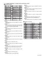
NOTE:

)

 (This mark shows where to attach the screws) : Do not reuse the screws because the screw lock bond was applied to prevent the 

screws from loosening. 


Prepare the specified screws and use them in place of the removed screws.

)Tightening torque for the screws

There are setting limits of the torque value for the torque driver. If the value exceeds the setting value, take it as a rough 

measurement (reference value),  


and tighten the screw manually. 

The specified torque value is a recommended value of the initial assembly. Therefore, set the value below the specified torque 

value in the assembling procedure.


Be careful not to break either the screws or the screw holes.

a

 0.069N

m (0.7kgf

cm)

ޓޓ

b

 0.059N

m (0.6kgf

cm) 

ޓޓ

c

 0.147N

m (1.5kgf

cm)

ޓޓ

d

 0.118N

m (1.2kgf

cm)

ޓޓ

e

 0.078N

m (0.8kgf

cm)

 0.198N

m (2.0kgf

cm)

ޓޓ

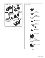
[8] UPPER CASE ASSY

[17] MONITOR ASSY

 [16]VF ASSY

[9]

OP BLOCK ASSY/CCD BOARD ASSY

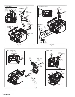
CABINET PARTS AND ELECTRICAL PARTS(1)

CABINET PARTS AND ELECTRICAL PARTS(2)

[3]

[4]

FA2

FA1

aa

a

ee

f

c

a

a

a

a

FA3

[8]

456789

1

0

2

13

4567

2

13

11

456789

1

0

2

1

3

11

12

12

43

44

46

40

41

42

48

35

27

[1]

[2]

[5]

[6]

[7]

FA4

FA5

38

39

30

29

28

31

32

33

34

35

36

37

FA5

U1

VF1

VF2

U2

U3

3-2-6

3-2-4

FA7

FA8

FA9

FA10-1

[9]

[10]

[11]

[12]

[13]

[14]

[15]

[18] 

[17] 

[16] 

[16] 

[17] 

[9] 

2

1

456789

1

0

3

1

11

21

31

41

51

61

7

1

92

02

12

22

32

42

52

6

18

4

47

45

b

b

b

a

d

Содержание GR-DF420EK

Страница 1: ...70EY GR DF470EZ For disassembling and assembling of MECHANISM ASSEMBLY refer to the SERVICE MANUAL No 86700 MECHANISM ASSEMBLY TABLE OF CONTENTS 1 PRECAUTIONS 1 3 2 SPECIFIC SERVICE INSTRUCTIONS 1 5 3 DISASSEMBLY 1 6 4 ADJUSTMENT 1 17 5 TROUBLE SHOOTING 1 20 GR DF420EKM GR DF420EXM GR DF420EYM GR DF420EZM GR DF425EKM GR DF425EGM M5D5S2 GR DF430EKM M5D5S3 GR DF460EKM M5D5S6 GR DF470EKM GR DF470EXM ...

Страница 2: ... m For Digital Video Camera Format DV format SD mode Signal format PAL standard Recording Playback format Video Digital component recording Audio PCM digital recording 32 kHz 4 channel 12 bit 48 kHz 2 channel 16 bit Cassette Mini DV cassette Tape speed SP 18 8 mm s LP 12 5 mm s Maximum recording time using 80 min cassette SP 80 min LP 120 min For Digital Still Camera GR DF460 470 only Storage medi...

Страница 3: ...rts 9 When a power cord has been replaced check that 10 15 kg of force in any direction will not loosen it Fig 1 1 2 10 Also check areas surrounding repaired locations 11 Products using cathode ray tubes CRTs In regard to such products the cathode ray tubes themselves the high voltage circuits and related circuits are specified for compliance with recognized codes pertaining to X ray emission Cons...

Страница 4: ...g prongs and externally exposed accessible parts Use an AC voltmeter to measure across both terminals of load Z See Fig 1 1 9 and following Fig 1 1 12 Fig 1 1 9 5 Grounding Class 1 model only Confirm specified or lower grounding impedance between earth pin in AC inlet and externally exposed accessible parts Video in Video out Audio in Audio out or Fixing screw etc Measuring Method Connect milli oh...

Страница 5: ...L NAME GR DF425EK GR DF425EG GR DF430EK GR DF460EK LED LIGHT NO NO NO YES MEMORY CARD NO NO NO MMC 8MB USB TERMINAL NO NO NO USB VC DV TERMINAL YES OUT YES OUT YES IN OUT YES OUT ANALOG INPUT NO NO YES NO REMOTE CONTROL NO RM V720US RM V720US RM V720US VIDEO MEMORY NO NO NO YES AC ADAPTER AP V14E AP V17E AP V14E AP V14E AC CORD YES BS Plug NO YES BS Plug YES BS Plug USB CABLE NO NO NO YES CD ROM Y...

Страница 6: ...er 1 Order of steps in Procedure When reassembling preform the step s in the reverseorder These numbers are also used as the identification location No of parts Figures 2 Part to be removed or installed 3 Fig No showing Procedure or Part Location 4 Identification of part to be removed unhooked unlocked released unplugged unclamped or unsoldered S Screw L Lock Release Hook SD Solder CN Connector Ex...

Страница 7: ...he EJECT SW NOTE13a During the procedure be careful in handling the HEAT SINK1 NOTE13b Be careful with the wiring and the handling of the wire Pay special attention for the wire folding position NOTE15 When attaching be careful not to catch the FPC in between zDestination of connectors 1 2 3 4 5 6 7 8 9 10 11 12 13 14 15 COVER JIG CON COVER TOP ASSY SHOE CENTER COVER REAR COVER ASSY FRONT COVER N ...

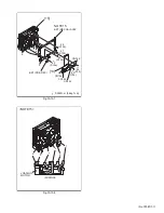
Страница 8: ...1a NOTE1b NOTE1c NOTE1b JACK COVER DV JACK COVER DV CASSETTE COVER 3 7 S4 10 S4 9 S4 8 S4 4 S3 5 S3 6 S3 9 S4 10 S4 4 BOTTOM VIEW NOTE4 L4 L5a L5b VF 14 S5b 14 S5b A 5 A CN5 JACK COVER DC NOTE5 NOTE5 15 S5c 15 S5c 16 S5d 16 S5d 12 S5a 12 S5a 11 S5a 11 S5a 13 S5a 13 S5a BOTTOM VIEW ...

Страница 9: ...YF087 1 9 Fig FA4 Fig FA5 BKT FRONT 6 7 WIRE MIC NOTE7 NOTE6a NOTE6b NOTE6b 19 S6b 20 S6b 21 S6b 21 S6b 22 S7 23 S7 17 S6a 18 S6a CN6 CN6 BOTTOM VIEW WIRING 24 S8a 26 S8c 27 S8c 25 S8b CN8 L8a L8b 8 8 NOTE8 ...

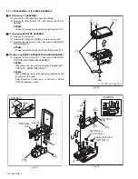
Страница 10: ...E E 10 E E NOTE10b NOTE10a NOTE10c CN10a HEAT SINK1 WIRE JACK COVER MIC 12 11 37 S11b 38 S12 36 S11a 35 S11a 34 S11a NOTE11a NOTE11b NOTE11c NOTE12 GRIP BELT a a L12b L12a EJECT SW G 13 F F G L13a 39 S13a 40 S13a 41 S13a 42 S13b CN13a L13b L13c CN13b CN13c H FPC SENSOR FPC CN13b G H HEAT SINK1 NOTE13a NOTE13b SHIELD PLATE 0 059N㨯m 0 6kgf㨯cm ...

Страница 11: ...87 1 11 Fig FA10 1 Fig FA10 2 46 S15b 47 S15b 48 S15b 45 S15a 43 S14 44 S14 14 15 CN14a CN14b CN14c CN14d a a b c d 0 059N㨯m 0 6kgf㨯cm NOTE15 BKT PRE REC BKT MECHA ASSY a b c d e f WIRING LOADING MOTOR NOTE15 ...

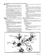
Страница 12: ...ful not to break the FPC z 18 Removing MONITOR OPERATION BOARD ASSEMBLY 1 Remove the five screws 7 11 and remove the MONI TOR OPERATION BOARD ASSEMBLY NOTE8c When removing be careful in handling the parts BUT TON SET KNOB VIDEO DSC NOTE8d When attaching be careful with the positions and the directions of the parts After attachment make sure to perform a SLIDE SWITCH operation check Fig U1 Fig U2 F...

Страница 13: ... ASSEMBLY In replacing the CCD IMAGE SENSOR don t remove the CCD IMAGE SENSOR from the CCD BASE AS SEMBLY Instead replace the whole CCD BASE AS SEMBLY NOTE9c Since the OP LPF is inside the LPF HOLDER and the OP LPF is attached to the LPF HOLDER by using the SHEET remove the OP LPF from the LPF HOLDER if necessary In removing the OP LPF from the LPF HOLDER be careful not to damage the LPF HOLDER an...

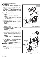
Страница 14: ...nd remove the FPC which is affixed to the back of the HOLDER SW 6 Remove the two hooks L16k m from both sides and remove the UPPER CASE VF NOTE16d When attaching be careful with the positions of the KNOB ADJ and the LENS ASSY Make sure to check the slide operation 7 Remove the FPC from the CASE LOWER to free the FPC and remove the LCD ASSEMBY LENS ASSEM BLY NOTE16e During the procedure be careful ...

Страница 15: ...16q CASE LOWER LENS ASSY LCD ASSY COVER LENS CASE UPPER KNOB ADJ NOTE16d e NOTE16g NOTE16d NOTE16d NOTE16f CASE B LIGHT SHEET DIFF SHEET POLA 1 CUSHION LCD LCD MODULE GUIDE LCD HOLDER LCD SHEET POLA 2 STOPER POLA L16s L16t L16u L16r LCD ASSY NOTE16h NOTE16h NOTE16h NOTE16h ...

Страница 16: ... attaching make sure to place the CN17b under 4 Release the lock of the connector CN17c and pull out the FPC 5 Remove the screw 5 6 Remove the MONI BL BOARD ASSEMBLY and the BACK LIGHT together NOTE17d Since the BACKLIGHT is soldered to the BOARD AS SEMBLY SD17 they should be removed together except for the replacement 7 Remove the SHEET DIFF and the SHEET BEF 8 Remove the LCD MODULE 9 Remove the ...

Страница 17: ... 100MHz or higher frequency The one observable 300 MHz or higher frequency is recommended Digital voltmeter DC power supply or AC adapter Frequency counter with threshold level adjuster 4 1 3 TOOLS REQUIRED FOR ADJUSTMENT Chip IC replacement jig To be used for adjustment of the camera system Cleaning cloth Recommended the Cleaning cloth to wipe down the video heads mechanism tape transport system ...

Страница 18: ...the Videocamera and a personal computer with each other when a personal computer issued for adjustment Communication cable Connect the Communication cable between the PC cable and Jig connector cable when performing a PC adjustment Service support system To be used for adjustment with a personal computer Software can be downloaded also from JS net Jig connector cable Connected to JIG CONNECTOR of ...

Страница 19: ...nfirm that the waveform is flat when the tape has been played back again 7 Play back the self recording 8 Confirm that the waveform is flat Fig 4 3 1 Fig 4 3 2 4 4 ELECTRICAL ADJUSTMENT Electrical adjustment is performed by using a personal computer and software for SERVICE SUPPORT SYSTEM Read README TXT file to use the software properly As for the connection of cables see 4 2 JIG CONNECTOR CABLE ...

Страница 20: ...lue exceeds the setting value take it as a rough measurement reference value and tighten the screw manually The specified torque value is a recommended value of the initial assembly Therefore set the value below the specified torque value in the assembling procedure Be careful not to break either the screws or the screw holes a㧦 0 069N㨯m 0 7kgf㨯cm ޓޓ b㧦 0 059N㨯m 0 6kgf㨯cm ޓޓ c㧦 0 147N㨯m 1 5kgf㨯cm ...

Страница 21: ...ell 2 Though the idler gear and reel disk are engaged with each other the tape is not wound because of overload to the mechanism 3 No FG pulse is output from the reel sensor 4 No power is supplied to the reel sensor 5 Tape transport operation takes place with a cassette having no tape inside 6 The tape slackens and no pulse is produced until the slack is taken up and the tape comes into the normal...

Страница 22: ... No YF087 AV MULTIMEDIA COMPANY CAMCORDER CATEGORY 12 3 chome Moriya cho kanagawa ku Yokohama kanagawa prefecture 221 8528 Japan Victor Company of Japan Limited VPT Printed in Japan ...

Страница 23: ... GR DF420EZ GR DF425EK GR DF425EG GR DF430EK GR DF460EK GR DF470EK GR DF470EX GR DF470EY GR DF470EZ GR DF420EKM GR DF420EXM GR DF420EYM GR DF420EZM GR DF425EKM GR DF425EGM M5D5S2 GR DF430EKM M5D5S3 GR DF460EKM M5D5S6 GR DF470EKM GR DF470EXM GR DF470EYM GR DF470EZM M5D5S7 SCHEMATIC DIAGRAMS No YF087SCH CD ROM No SML200503 ...

Страница 24: ... signal path including E E signal path Capstan servo path Drum servo path Example R Y Y Playback R Y signal path Recording Y signal path 6 Indication of the parts for adjustments The parts for the adjustments are surrounded with the circle as shown below 7 Indication of the parts not mounted on the circuit board OPEN is indicated by the parts not mounted on the circuit board R216 OPEN 1 2 3 1 2 3 ...

Страница 25: ... MMC_DOUT MMC_CS DOLRCK2 AIMCK DOMCK2 DOBCK2 DODAT2 AODAT AIDAT12 AILRCK DOLRCK2 AIBCK DOBCK2 AIMCK AODAT AIDAT12 DODAT2 DOLRCK2 AIMCK DOBCK2 AIBCK DOBCK2 AILRCK DOLRCK2 AIMCK DOMCK2 AIDAT AIDAT2 AODAT AILRCK S_SHUT AIBCK AIMCK AU_LV_OUT AU_LV_CLK L_MUTE BINAURAL_H BUZZER SHUT_ATT PD_L A_MUTE AUDIO_CS EM_DET_L BUZZER L_MUTE AU_LV_CLK SHUT_ATT AU_LV_OUT A_MUTE EM_DET_L PD_L AUDIO_CS BINAURAL_H 14 1...

Страница 26: ...LAMP_ON MIC1 IR_OUT REC_SAFE T_RL EJT_SW S_SENS MIC2 E_SENS GND T_RL REG_3 1V REG_4 8V TAPE_LED S_RL R2004 0Ω EM_DET_L GND EXT R EXT L QGF0530F3 16W 1 2 3 4 5 6 7 8 9 10 11 12 13 14 15 16 REG_4 8V REG_4 8V REG_4 8V REG_3 1V VFREG4 8 GND GND GND GND GND MENU_SW SET_SW KEY_A KEY_C MONI_SW LITHIUM C_OUT Y_OUT S_DET REG_3 1V ZOOM_SW GND GND QGF0528F1 40X TO REAR CN501 1 2 3 4 5 6 7 8 9 10 11 12 13 14 ...

Страница 27: ...N 184 LCD_CS 148 IRIS_MCK 128 USB_STS 83 FLD 205 FRMREF 134 TRKREF 174 SRVTRK 133 SPA 26 DRUM_PG 16 PD_L 132 S_REEL 84 T_REEL 147 ROM_CS 183 VF_CS 28 CAP_FG 27 DRUM_FG 196 ASPECT1 160 ASPECT2 72 L_MUTE 124 A_MUTE 220 RGB_CTL 222 XINT 194 JLIP_INT 193 CHG_WKUP 223 DSC_CS 65 OMT 130 OUTV 64 VD 92 P_MEDIA 49 TVSEL 214 CHRG_EVR 48 CAP_PWM 44 DRUM_PWM 67 EEP_CLK 197 EEP_OUT 224 EEP_IN 19 TRIG_OUT 198 T...

Страница 28: ... Q2201 DTC144EE X A_MUTE T C2401 10 6 3 T C2402 10 6 3 R2609 22k C2610 0 0033 L_MUTE R2204 150k C2611 1 C2656 0 047 R2207 33k DOLRCK2 AIMCK DOMCK2 DOBCK2 DODAT2 C2623 10p C2624 10p R2206 33k R2211 820 R2233 560k Q2202 UMX1N W 2 1 4 5 3 6 R2235 3 3k R2210 820 R2234 560k C2225 OPEN C2226 OPEN C2227 OPEN C2228 OPEN C2229 OPEN SN74LV4053ARG X C2233 OPEN C2234 OPEN C2235 OPEN IC2801 16 15 14 13 12 11 1...

Страница 29: ...VCC 320 ADD_VSS 319 ADD_VDDE 151 CLK24O 154 VCC 58 DSYO0 241 DSYO1 59 DSYO2 242 DSYO3 155 DSYO4 60 DSYO5 321 DSYO6 322 DSYO7 243 VCC 156 ADD_VSS 61 ADD_VDDE 244 DSCO0 157 DSCO1 324 DSCO2 323 DSCO3 62 DSCO4 245 DSCO5 158 DSCO6 63 DSCO7 64 ADD_VDDL 159 ADD_VSS 246 ADD_VDDE 65 DSYIO0 325 DSYIO1 328 DSYIO2 160 DSYIO3 247 DSYIO4 66 DSYIO5 161 DSYIO6 248 DSYIO7 327 ADD_VSS 67 ADD_VDDE 326 DSCIO0 162 DSC...

Страница 30: ... 123 VDD 8AD 38 VSS 8AD 85 VSS 171 NC 172 NC 173 NC 174 NC 175 NC 53 NC 64 NC 75 NC 86 NC 154 VCCQ 87 CSI0 42 CSI1 124 VSSQ 125 CSI2 88 CSI3 155 VCCQ 43 VDD I O 126 CSI4 89 VSS 44 VDD CORE 127 CSI5 156 VSSQ 90 CSI6 45 CSI7 128 INH 91 INV 46 VDD CORE 157 VSS 129 VDD I O 158 VCC 47 VSS 92 YSI0 48 VDD CORE 93 YSI1 130 VSSQ 49 YSI2 94 YSI3 131 VCCQ 50 YSI4 95 YSI5 159 VSSQ 132 YSI6 51 YSI7 96 VDD I O ...

Страница 31: ...01X L3504 NQR0006 001X GND L3502 NQL402M 100X REG_4 8V REG_3 1V IC3502 OPEN 1 2 3 4 5 R3501 470 R3502 100k R3503 1k R3504 240 R3505 240 R3506 240 R3507 240 R3508 22k R3509 OPEN R3510 OPEN R3512 0Ω C3526 0 01 C3504 0 047 C3505 0 022 C3506 1 C3507 0 01 C3508 0 01 C3509 0 01 C3510 0 1 C3511 0 01 C3512 0 1 C3513 0 1 C3514 0 047 C3515 0 047 C3516 0 047 C3517 OPEN C3518 0 01 C3519 0 001 C3520 0 01 C3521...

Страница 32: ... 0 1 C4207 1 VDIN HDIN ID CPOB PBLK CLKI R4201 33k C4201 0 1 C4202 1 L4202 10µ T C4216 22 6 3 C4217 0 1 L4201 NQR0129 002X GND REG_4 8V REG_3 1V REG_15V REG CCD R5506 10 R5507 10 R5508 10 L5507 10µ C5518 0 1 T C5519 10 6 3 C5504 0 1 T C5515 47 4 C5512 0 1 C5509 0 1 L5501 10µ L5502 NQR0129 002X R5501 1k R5502 1k R5503 1k R5504 10 R5505 10 R5510 100k C5501 0 1 C5502 0 1 C5503 0 1 C5507 0 1 C5505 0 1...

Страница 33: ...SDATA 10 SCLK 11 OSCIN 12 RESET 13 VCC5D 14 GND5D 15 VSEN_LA 16 VSEN_HA 17 A1 N1 18 VMD 19 NC 20 NC 21 ORSA 22 A2 N3 23 B1 N2 24 ORSB 25 B2 N4 26 VMB 27 VSEN 28 VSEN_LB 29 NC 30 NC 31 NC 32 NC 33 VSEN_LC 34 VSEN_HC 35 VMC 36 C2 W3 37 ORSC 38 C1 W1 39 D2 W4 40 ORSD 41 NC 42 NC 43 VMD 44 D1 W2 45 VSEN_HD 46 VSEN_LD 47 GND5A 48 VCC5A ATF_GAIN R4924 12k M_VCOCTL PBVCOCTL IC4901 1 2 11 54 12 13 22 63 2...

Страница 34: ...C6303 0 068 DRUM_ERR D_GAIN REG CCD R6404 47k R6403 27k C6403 1 CAP_ERR R6010 1k C6507 OPEN D6502 RB480Y W 1 2 3 4 D6001 RB715W X 2 1 3 AL_3 1V GND LIT_3V CHRG_EVR L6502 NQL38DK 100X C6504 OPEN REG_3 1V C6704 0 0047 R6714 4 7k TL6001 R6709 110k C6703 OPEN R6708 15k R6716 8 2k R6715 4 7k R6513 2 7k C6204 220p R6204 8 2k R6512 47k C6509 0 033 R6103 8 2k R6802 4 7k R6104 R6803 1k C6104 680p C6804 0 0...

Страница 35: ...D24 103 SDR_DQ23 ARM_D23 102 SDR_DQ22 ARM_D22 101 SDR_DQ21 ARM_D21 99 SDR_DQ20 ARM_D20 93 SDR_DQ19 ARM_D19 100 SDR_DQ18 ARM_D18 91 SDR_DQ17 ARM_D17 76 SDR_DQ16 ARM_D16 75 SDR_DQ15 90 SDR_DQ14 74 SDR_DQ13 61 SDR_DQ12 60 SDR_DQ11 55 SDR_DQ10 59 SDR_DQ9 54 SDR_DQ8 36 SDR_DQ7 53 SDR_DQ6 35 SDR_DQ5 17 SDR_DQ4 34 SDR_DQ3 16 SDR_DQ2 33 SDR_DQ1 15 SDR_DQ0 195 SDR_DQMHH 178 SDR_DQMHL 160 SDR_DQMLH 180 SDR_...

Страница 36: ...SREQ xEPIWAIT 50 xEPIIRQ 13 xEPIWR 51 xEPIRD 102 xEPICS 53 HVDD 103 VSS 52 EPID0 14 EPID1 81 EPID2 82 EPID3 15 EPID4 16 EPID5 104 EPID6 83 EPID7 17 EPID8 106 EPID9 54 EPID10 55 EPID11 18 EPID12 56 EPID13 19 EPID14 85 EPID15 20 EPIA0 57 EPIA1 21 NC 22 EPIA2 58 EPIA3 84 LVDD 105 VSS 59 LVDD 23 PDIR 86 PMSYNC 24 PMACK 87 PMREQ PSRD 88 EXTFRP 25 EXTACCESS 60 EXTREQ 26 EXTCLK 61 HVDD 107 VSS 89 EXTD0 2...

Страница 37: ... 6 SUB 7 RG 8 CCD_ 7 5V 9 CCD_ 7 5V 10 GND 11 GND 12 GND 13 CCD_OUT 14 GND 15 GND 16 GND 17 V1 18 V2 19 V3 20 V4 IC5001 ICX440UKM V 1 6 Inch_CCD Top View 14 TEST 13 H2 12 H1 11 VL 10 SUB 9 RG 8 Vdd 7 Vout 6 GND 5 GND 4 V1 3 V2 2 V3 1 V4 Q5002 1 2 3 2SC4081 QR X 2SC3931 CD X 1 2 3 Q5001 C5002 0 1 C5005 0 1 C5007 2200p C5004 0 1 T C5001 4 7 25 T C5003 10 16 L5001 10µ L5002 10µ R5001 4 7k C5006 0 1 R...

Страница 38: ...K R50 F1601 NMFZ007 R20X K R20 R1611 390 R1610 390 D1604 DAP222 X C1632 0 47 L1601 NQL382M 100X 10 R1617 0 33 TL1617 TL1619 TL1613 TL1618 TL1612 TL1620 TL1602 TL1601 TL1607 C1618 0 0022 C1619 0 0022 C1620 0 0022 C1616 Q1601 UMC3N W C1635 CN301 1 HG_U 2 HG_V 3 HG_W 4 HG_BS 5 HG_BS 6 HG_W 7 HG_V 8 HG_U 9 C_COIL_V 10 C_COIL_V 11 C_COIL_U 12 C_COIL_U 13 C_COIL_W 14 C_COIL_W 15 MDA_2 9V 16 C_FG 17 GND ...

Страница 39: ...MMC 3 VSS GND 4 VDD DSC_3V 5 MMC_CLK 6 VSS2 CD 7 Dat2Host 8 SD_DATA1 T C902 10 6 3 C903 OPEN GND SD_WP MMC_DIN MMC_DOUT MMC_CD MMC_CLK REG_3 1V MMC_CS D503 UDZS6 8B X L501 NQR0251 004X C501 0 01 L503 NQR0251 004X C503 OPEN J502 QNS0078 001 1 2 3 5 4 7 R501 100 C504 OPEN C502 0 01 L502 NQR0251 004X R502 100 AU_SIG R P_DET V_OUT AU_SIG L GND TP2 T TP3 D TP1 TP4 J501 QNA0039 001 4 5 3 6 2 ADP_L GND A...

Страница 40: ...AIN IF CN107 FRONT SCHEMATIC DIAGRAM NOTES 1 For the destination of each signal and further line connections that are cut off from this diagram refer to BOARD INTERCONNECTIONS 2 The parts with marked is not used S607 STOP 3 1 2 4 J601 QND0078 001 1 2 3 4 5 NC 6 D601 MA8068 X Y_OUT C_OUT S_DET S602 NSW0161 001X 1 2 S601 NSW0099 001X 1 2 3 GND S608 REW 3 1 2 4 S610 PB 3 1 2 4 S609 FF 3 1 2 4 S611 SE...

Страница 41: ... 2 1 4 5 3 6 R7814 OPEN C7827 1 Q7805 PUMX1 W 2 1 4 5 3 6 R7816 20k R7815 4 7k R7817 OPEN C7828 1 C7824 4 7 16 C7819 4 7 16 R7806 100 R7805 100 CN601 1 C_OUT 2 LITHIUM 3 S_DET 4 Y_OUT 5 MONI_SW 6 KEY_C 7 KEY_A 8 SET_SW 9 MENU_SW 10 P_MEDIA 11 VF_SW 12 HST 13 HRP1 14 CVF_B 15 CVF_G 16 CVF_R 17 REG_12V 18 MON_B 19 MON_G 20 RGB_CTL 21 GND 22 GND 23 GND 24 GND 25 GND 26 GND 27 HRP2 28 VFREG4 8 29 REG_...

Страница 42: ...702 1K Q7703 2SD1664 R7701 1K T7701 NQS0062 001X 6 10 5 1 3 2 4 C7705 18p F7701 NMFZ007 R40X K C7702 0 01 JP7702 C7703 0 027 L7701 Q7704 2SD1664 C7701 10 L7702 JP7705 JP7704 JP7706 R7757 10 R7758 10 R7759 10 R7760 OPEN CN702 1 REG_4 8V 2 REG_4 8V 3 LCD_CTL 4 BL_GND 5 BL_GND 6 LV_CLK 7 LV_OUT 8 M_CS 9 M_RVS 10 MON_B 11 MON_G 12 MON_R CN701 1 REG_4 8V 2 VD 3 HD 4 HRP1 5 REG_3 1V 6 REG_3 1V 7 REG_3 1...

Страница 43: ... HST 10 HCK2 11 HCK1 12 VIDB 13 VIDG 14 VIDR 15 VCOM R7105 56k C7105 OPEN R7107 4 7k 1 CVF_R 2 CVF_G 3 CVF_B 4 HCK1 5 HCK2 6 HST 7 VCK 8 VST 9 EN 10 VF_SLEEP 11 VF_9V 12 VFREG4 8 13 GND 14 GND C7102 0 1 VF 8 0 CN7101 TO MONI OPE CN603 TO 0 33 LCD MODULE VF SCHEMATIC DIAGRAM NOTES 1 For the destination of each signal and further line connections that are cut off from this diagram refer to BOARD INT...

Страница 44: ...Q8601 D6001 D6501 D3701 IC8102 IC3731 RA3201 RA3202 RA8607 L6201 X8601 CN114 IC6001 1 16 17 32 33 48 49 64 IC8601 IC8001 IC8003 IC8002 1 43 44 86 Q6703 D6702 L3204 L3701 L4955 L6502 L1701 L1702 C1703 R8627 R3098 C8618 R2235 R2402 R2403 R2601 R2602 R2607 R2608 R2618 R2619 R3201 R3202 R3204 R3205 R3701 R3703 R3704 R3707 R3712 R3713 R3715 R3722 R3724 R3725 R3726 R3727 R3728 R3730 R3731 R3732 R3735 R3...

Страница 45: ... IC1005 1 4 5 8 IC2201 1 12 13 24 25 36 37 48 IC3501 1 1 45 44 8 16 17 32 33 48 49 64 IC3001 IC1001 IC4901 IC4201 1 1 2 19 20 18 19 36 CN113 CN109 Q3501 L3001 L3004 L4902 L4954 L5501 CN106 CN105 R2004 R1065 R1109 R1101 R1108 Q1008 R1040 R5511 TL1021 TL3001 TL3002 TL3003 TL3004 TL3005 TL3006 TL3007 TL3008 TL3015 TL4201 TL4202 R1001 R1003 R1005 R1007 R1008 R1012 R1013 R1016 R1017 R1018 R1019 R1022 R...

Страница 46: ...Q7804 Q7805 1 24 45 1 1 2 15 16 S606 S607 S608 S609 S610 S611 J601 R601 R602 R604 R605 BT601 C7802 C7804 C7805 C7807 C7817 C7823 C7806 C7815 C7818 IC7801 1 12 13 24 25 36 37 48 R7804 R7836 R7837 R7838 R7839 R7840 R7842 R7843 S603 S604 S605 S602 IC7802 1 3 5 4 S601 R606 R7806 C7816 C7819 C7821 C7822 C7812 C7813 C7814 L7804 R7803 R7805 R7835 R7841 C7832 C7831 R7701 R7702 R7754 R7755 R7756 R7757 R775...

Страница 47: ...CC F_LED MONI BL 0 7 34 29 27 21 3 1V REG Q6101 REG_3 1 V REG_12V IC8005 1 9V REG REG_3 1V REG_1 7V IC3701 IC3731 Q3702 Q3731 Q3733 Q3734 Q3735 IC3201 VIDEO REG_4 8V REG_2 5V REG_3 1V REG_1 7V Q3001 IC3001 PARAGON REG_4 8V REG_2 5V 22 5 VF_9V VFREG4 8 CN7101 CN7102 11 12 2 VF LCD MODULE CVF Q7101 D7101 CN108 3 REG_4 8V REG_4 8V 15 14 REG_4 8V 14 2 3 CN107 CN401 IC401 Q401 1 2 CN112 9 4 9 4 CCD 7 5...

Страница 48: ...CO 0 7 REC_DATA ATFI TPA TPB T_F_V_RST CAM_CLK CAM_OUT RTC_IN VOI_CLK VOI_OUT OSD_CS EEP_IN EEP_OUT DSC_CLK DSC_RST DSC_CS H1 H2 V1 V4 CN5001 CN5001 CN101 CN901 CN501 3 2 1 CN603 CN7101 CN7102 CN109 14 17 1 4 T_F_V_RST IRIS_CS IRIS_PS 2S 2F 1S 1F A 13 16 D 0 15 13 13 CCD_OUT H1 H2 1 8 33 CN103 AGC_OUT TG_CS T_F_V_RST CAM_CLK CAM_OUT PARAGON IC3001 EXTDATA 0 7 TO IC8601 USB DRIVER EXTDATA 0 7 TO IC...

Страница 49: ...0 0 66 0 0 67 0 0 68 0 0 69 0 0 70 0 0 71 0 0 72 0 0 73 0 0 74 0 0 75 3 0 3 1 76 0 0 77 0 0 78 0 0 79 0 0 80 0 0 81 3 0 3 0 82 0 0 83 0 0 84 0 0 85 0 0 86 0 0 IC8003 IC8005 1 3 0 3 1 2 0 0 3 3 0 2 9 4 0 0 5 1 8 1 7 IC8101 1 0 9 0 9 2 0 0 3 0 0 4 0 0 5 0 8 0 9 6 0 0 7 0 3 0 3 8 0 6 0 7 9 0 0 10 0 0 11 0 0 12 0 9 0 9 13 0 0 1 14 0 2 0 3 15 0 0 16 0 0 2 IC8102 1 1 4 1 3 2 0 0 3 0 0 4 0 0 5 3 0 3 0 6 ...

Страница 50: ... No YF087 AV MULTIMEDIA COMPANY CAMCORDER CATEGORY 12 3 chome Moriya cho kanagawa ku Yokohama kanagawa prefecture 221 8528 Japan Victor Company of Japan Limited VPT Printed in Japan ...

Страница 51: ... W1 c F1 F2 F3 F4 F5 101 114 114 114 115 102 a F7 b 119 119 119 119 F8 F9 c 101A 101A 101A e 109 108 124 124 126 107A 107B 107D 107D 107D 107C 125 107 128 128 REAR BOARD ASSEMBLY 05 111 MEMORY CARD WITHOUT 140 140 139 140 140 142 113 135 135 135 112 f g g 131 129 130 F13 h h h WITH MEMORY CARD 136 136 k k m m 203 201 202 209 n n 210 o 208 207A 207 139B 139A 205 204 110D 110H 110H 110H 110A 110B 11...

Страница 52: ...LY MAIN BOARD 141 F8 F9 W1 145 121 120 121 147 F10 F10 d d 120 106A e 106B 106B 106B 106C 106C 106C 106 F11 F11 122 137 137 127 127 133 133 132 F12 F12 f F13 o 206 607 601D 601A 601D 601B 601D 601D 601C 601E 601E 601F 603 602 608 604 605 601 607 120 601 123 ASSEMBLY UPPER CCD BOARD ASSEMBLY 02 610 609 ...

Страница 53: ...ONT BOARD 328 324 327 326 325 325 323 a a 301AB 301AD 301T 301AC 301S 301Z 301H 301D 301A 301B 301V 301AA 301N 301M 301S 301J 301Q 301G 301AE 301W 301X 301K 301P 327A 301U 301E 301F 301V 301Y 301L 301S 301C 301 301R 300 301AF 301T ...

Страница 54: ...05 519 510 509 508 507 506 a a F1 F2 F3 F2 F3 520 520 521 513 521 507A 507A 513A d d 523 523 514 524 b b 515 525 525 MONI OPE BOARD ASSEMBLY 06 526 526 528 526 526 527 518 529 529 530 514A 514B 523 538 538 533 534 535 537 536 515B 515B 515A 532 c c 517 500 599 ...

Страница 55: ...33 932 947 948 946 966 945 944 959 958 960 941 957 955 952 953 953 931 937 937 925 924 937 928 929 954 935 961 963 965 BB AA AA AA CC AA CC CC CC CC AA AA 930 AA 976 979 934 900 AA 936 YMA0029AB YMA0029BU 998 CC JVS 306U Grease BB is not contained in 900A NOTE2 Mark indicate lubrication and greasing areas NOTE1 The section marked in AA BB and CC YTU94027 Oil AA KYODO SH JB Grease Symbol in drawing...

Страница 56: ...3 6 No YF087 1 3 VF COLOR ASSEMBLY M3 710 709 708 707 711 705 706 703 704 713 712 VF BOARD ASSEMBLY 08 799 b 714 715 716 717 718 725 720 724 721 719 723 728 728 726 722 727 727 a a b 700 ...

Страница 57: ... No YF087 3 7 1 5 PACKING AND ACCESSORY ASSEMBLY M5 012 013 014 067 054 LABEL SERIAL FINAL ASSEMBLY M1 070 066 059 055 071 062 060 001 021 003 002 053 065 072 022 052 068 069 061 063 005 004 058 051 ...

Страница 58: ...04E LOWER UNIT ASSY A B C D E F G 301 LY21364 001F LOWER UNIT ASSY H J K L M 301A LY21362 001B POWER UNIT 301B LY10563 001C ARM 301C LY21365 001A BKT ARM TOP 301D LY21366 001C BKT ARM BOTTOM 301E LY21367 001C PLATE2 ARM LOCK 301F LY30001 032A TENSION SPRING 301G LY34852 001A BKT LOWER 301H LY10564 001D LOWER CASE 301J LY10565 001D C COVER TOP A B C D E F G 301J LY10565 004C C COVER TOP H J K L M 3...

Страница 59: ...01C LOADING PLATE ASSY 943 YQ44246 SLIT WASHER 944 LY32858 001B EJECT LEVER 945 YQ44246 SLIT WASHER 946 LYH40271 001A BASE R ASSY Symbol No Part No Part Name Description Local 947 YQ43893 MINI SCREW 948 LY41945 001C MINI SCREW 949 LY43665 001A MODE GEAR 950 QSW0876 005 ROTARY ENCODER 951 YQ43893 MINI SCREW x2 952 LY32860 001E GEAR COVER ASSY 953 YQ43893 MINI SCREW x2 954 LY43675 007A MINI SCREW 95...

Страница 60: ...002 CORE FILTER AV 058 QAM0495 001 AUDIO CABLE MIC 059 QQR0917 002 CORE FILTER MIC 2T 060 QAM0538 001 USB CABLE USB H J K L M 061 QQR0491 002 FERRITE CORE USB 1T TDK BLACK H J K L M 062 LY21104 001C AC ADAPTER AP V14E A F G H J 062 LY21343 001A AC ADAPTER AP V17E B C D E K L M 063 QQR0917 002 CORE FILTER DC Symbol No Part No Part Name Description Local 065 QAM0302 001 ADAPTOR PLUG PERI RCAS 066 LY...

Страница 61: ...ODE ARRAY D1001 or MA133 X SI DIODE D1002 1SS376 X SI DIODE D3001 RB551V 30 X SB DIODE PHY VDD D3002 EC2C01C TR X VARI CAP DIODE FS VCO D3003 EC2C01C TR X VARI CAP DIODE FS VCO D3004 EC2C01C TR X VARI CAP DIODE MAIN VCO D3005 DAN222 X SI DIODE D3005 or MA132WK X SI DIODE D5501 1SS355 X SI DIODE D5501 or MA111 X SI DIODE D6001 RB715W X SB DIODE D6501 RB480Y W SB DIODE D6502 RB480Y W SB DIODE D6701 ...

Страница 62: ...TOR 0 01uF 16V K C3071 NCBA1AK 104W C CAPACITOR 0 1uF 10V K C3072 NCBA1AK 104W C CAPACITOR 0 1uF 10V K C3073 NCBA1AK 104W C CAPACITOR 0 1uF 10V K C3201 NBE20JM 106X TA E CAPACITOR 10uF 6 3V M C3202 NCB21CK 105X C CAPACITOR 1uF 16V K C3203 NCB21CK 105X C CAPACITOR 1uF 16V K C3204 NBE20JM 106X TA E CAPACITOR 10uF 6 3V M C3205 NBE20GM 476X TA E CAPACITOR 47uF 4V M C3206 NCBA1CK 103W C CAPACITOR 0 01u...

Страница 63: ...1 NCB21CK 105X C CAPACITOR 1uF 16V K C6402 NCB21CK 105X C CAPACITOR 1uF 16V K C6403 NCB30JK 105X C CAPACITOR 1uF 6 3V K C6405 NCBA1CK 103W C CAPACITOR 0 01uF 16V K C6501 NCB21CK 105X C CAPACITOR 1uF 16V K C6502 NCB21CK 105X C CAPACITOR 1uF 16V K C6503 NCB21CK 105X C CAPACITOR 1uF 16V K C6505 NCB21CK 105X C CAPACITOR 1uF 16V K C6506 NCB21CK 105X C CAPACITOR 1uF 16V K C6508 NCB21CK 105X C CAPACITOR ...

Страница 64: ...rt Name Description Local R1090 NRSA6AJ 102W MG RESISTOR 1kΩ 1 16W J R1091 NRSA6AJ 102W MG RESISTOR 1kΩ 1 16W J R1092 NRSA6AJ 102W MG RESISTOR 1kΩ 1 16W J R1093 NRSA6AJ 102W MG RESISTOR 1kΩ 1 16W J R1094 NRSA6AJ 102W MG RESISTOR 1kΩ 1 16W J R1095 NRSA6AJ 102W MG RESISTOR 1kΩ 1 16W J R1096 NRSA6AJ 102W MG RESISTOR 1kΩ 1 16W J R1097 NRSA6AJ 102W MG RESISTOR 1kΩ 1 16W J R1098 NRSA6AJ 102W MG RESISTOR...

Страница 65: ...RSA6AJ 0R0W MG RESISTOR 0Ω 1 16W J R3214 NRSA6AJ 0R0W MG RESISTOR 0Ω 1 16W J R3501 NRSA6AJ 471W MG RESISTOR 470Ω 1 16W J R3502 NRSA6AJ 104W MG RESISTOR 100kΩ 1 16W J R3503 NRSA6AJ 102W MG RESISTOR 1kΩ 1 16W J R3504 NRVA6AD 241W CMF RESISTOR 240Ω 1 16W D R3505 NRVA6AD 241W CMF RESISTOR 240Ω 1 16W D R3506 NRVA6AD 241W CMF RESISTOR 240Ω 1 16W D R3507 NRVA6AD 241W CMF RESISTOR 240Ω 1 16W D R3508 NRSA6...

Страница 66: ...scription Local R8025 NRSA6AJ 472W MG RESISTOR 4 7kΩ 1 16W J H J K L M R8031 NRSA6AJ 100W MG RESISTOR 10Ω 1 16W J H J K L M R8032 NRSA6AJ 0R0W MG RESISTOR 0Ω 1 16W J H J K L M R8033 NRSA63J 0R0X MG RESISTOR 0Ω 1 16W J H J K L M R8036 NRSA6AJ 220W MG RESISTOR 22Ω 1 16W J H J K L M R8041 NRSA6AJ 220W MG RESISTOR 22Ω 1 16W J H J K L M R8042 NRSA6AJ 220W MG RESISTOR 22Ω 1 16W J H J K L M R8043 NRSA6AJ...

Страница 67: ... Name Description Local Q5002 2SC4081 QR X TRANSISTOR C5001 NBP41EM 475X B TA E CAPACITOR 4 7uF 25V M C5002 NCB31CK 104X C CAPACITOR 0 1uF 16V K C5003 NBP21CM 106X TA E CAPACITOR 10uF 16V M C5004 NCB31CK 104X C CAPACITOR 0 1uF 16V K C5005 NCB31CK 104X C CAPACITOR 0 1uF 16V K C5006 NCB31CK 104X C CAPACITOR 0 1uF 16V K C5007 NCB31HK 222X C CAPACITOR 2200pF 50V K R5001 NRSA63J 472X MG RESISTOR 4 7kΩ ...

Страница 68: ...JM 106X TA E CAPACITOR 10uF 6 3V M H J K L M R501 NRSA63J 101X MG RESISTOR 100Ω 1 16W J R502 NRSA63J 101X MG RESISTOR 100Ω 1 16W J R901 NRSA63J 103X MG RESISTOR 10kΩ 1 16W J H J K L M R902 NRSA63J 103X MG RESISTOR 10kΩ 1 16W J H J K L M R903 NRSA63J 103X MG RESISTOR 10kΩ 1 16W J H J K L M R904 NRSA63J 103X MG RESISTOR 10kΩ 1 16W J H J K L M R905 NRSA63J 103X MG RESISTOR 10kΩ 1 16W J H J K L M R906...

Страница 69: ... 001A E E CARD WIRE Symbol No Part No Part Name Description Local PW1 LYA10034 01B MONI BL BOARD ASSY IC7701 DN8797MS X IC Symbol No Part No Part Name Description Local Q7701 DTC144EE X DIGI TRANSISTOR Q7701 or BCR148T X DIGI TRANSISTOR Q7701 or UN9213J X DIGI TRANSISTOR Q7701 or PDTC144EE X DIGI TRANSISTOR Q7702 DTA144EE X DIGI TRANSISTOR Q7702 or BCR198T X DIGI TRANSISTOR Q7702 or UN9113J X DIGI...

Страница 70: ...16W D R7105 NRSA63D 563X MG RESISTOR 56kΩ 1 16W D R7106 NRSA63D 163X MG RESISTOR 16kΩ 1 16W D R7107 NRSA63D 472X MG RESISTOR 4 7kΩ 1 16W D R7108 NRSA63J 103X MG RESISTOR 10kΩ 1 16W J R7109 NRSA63J 103X MG RESISTOR 10kΩ 1 16W J CN7101 QGF0530F3 14W CONNECTOR MAIN FFC FPC 1 14 CN7102 QGF0530F3 15W CONNECTOR LCD FFC FPC 1 15 Symbol No Part No Part Name Description Local MODEL MARK A B C D GR DF420EK ...

Страница 71: ...Y OF JAPAN LTD No 86700 2003 04 MECHANISM ASSEMBLY 86700 2003 04 DVC MECHANISM VHS C MECHANISM VHS MECHANISM TABLE OF CONTENTS 1 JIGS AND TOOLS 1 1 2 SPECIFIC SERVICE INSTRUCTIONS 2 1 3 PARTS LIST 3 1 DVC MECHANISM VHS MECHANISM VHS C MECHANISM ...

Страница 72: ...screw thread 2 Bit This bit is slightly longer than those set in conventional torque drivers 3 Tweezers To be used for removing and installing parts and wires 4 Chip IC replacement jig To be used for replacement of part 5 Slit washer installation jig To be used to install slit washers 6 Cleaning cloth Recommended cleaning cloth to wipe down the video heads mechanism tape transport system optical l...

Страница 73: ... column corre spond to those appearing in drawings of this section 2 This column shows part names corresponding to numbers in the left column 3 The symbol T or B appearing in this column shows the side which the objective part is mounted on T the upper side B the lower side 4 Symbols appearing in this column indicate drawing num bers 5 This column indicates parts and points such as screws washers ...

Страница 74: ... into the C IN mode compulsory Mechanism assembly Cassette housing assembly Fig 2 1 1 Back side of the mechanism assembly Fig 2 1 2 2 1 3 2 Explanation of mechanism mode The mechanism mode of this model is classified into five modes as shown in Fig 2 1 9 Each mechanism mode can be distin guished from others by the relative position of marks on the sub cam gear to the inner or outer protrusion on t...

Страница 75: ... 177 79o 212 77o 243 94o 16 97o 30 71o 95 14o 110 06o 206 06o 210 05o 80 34o 0o 243 29o 291 16o 333 82o 292o 310o 74o L END LOCK OFF TU ARM ON OFF SLIDE DECK LOAD UL BRAKE S ON OFF BRAKE T ON OFF RELEASE LEVER ROTARY ENCODER MAIN CAM SUB CAM ON a OFF CTL PLATE C R L TENSION ARM UL L END OFF PAD ARM UL L END LOAD SUP L ARM UL L END LOAD TU L ARM UL PRESS LOAD P ROLLER UL b c C IN SHORT STOP PLAY RE...

Страница 76: ...N CTL PLATE ASSY T NOTE 18 ADJUSTMENT ADJUSTMENT BRAKE CTL LEVER ASSY T NOTE 19 ADJUSTMENT MOTOR BRACKET ASSY T Fig 2 1 21 NOTE 20 ADJUSTMENT GUIDE RAIL ASSY T NOTE 21 ADJUSTMENT SLIDE LEVER 2 ASSY T NOTE 22 ADJUSTMENT LOADING PLATE ASSY T NOTE 23 ADJUSTMENT MODE GEAR T NOTE 24 EJECT LEVER T NOTE 25 ADJUSTMENT BASE R ASSY T Fig 2 1 22 NOTE 26 ADJUSTMENT ROTARY ENCODER T NOTE 27 PHASE ADJUSTMENT GE...

Страница 77: ...8 23 22 17 16 19 12 14 11 5 4 1 S1 S3b 2 S1 W4 W12 P12 P8 P14 W14 W21 W23 W21 W25 W17 W6 W5a W5b 1 S10 11 S2 4 S1 3 S21 18 S20 17 S20 16 S20 15 S27 22 S35 27 S35 28 S36 30 S35 29 S32 26 S27 21 7 S11b 14 S11a 12 S11a 13 S3b 6 S26a 19 S28b 24 S28b 25 S28a 23 S3a 5 S6b 10 S6a 9 S6a 8 S26b 20 W15 ...

Страница 78: ...No 86700 Fig 2 1 12 Fig 2 1 13 TOP VIEW 5 24 27 2 3 36 35 21 26 17 34 9 10 33 26 6 25 11 32 37 14 31 28 16 15 30 29 4 12 7 8 22 18 23 20 19 34 26 32 31 16 6 30 30 25 36 3 22 27 20 37 18 29 11 19 BOTTOM VIEW ...

Страница 79: ...unting NOTE 1d When mounting be sure to locate the FPC in the gap Fig 2 1 14 2 1 5 2 2 UPPER BASE ASSY 3 DRUM ASSY NOTE 2 When mounting be sure to insert the FPC reinforcing sheet NOTE 3a Be mindful of scratches or damage during work NOTE 3b Be careful not to attach screws incorrectly Fig 2 1 15 NOTE 1b NOTE 1c LOCK LEVER EJECT LEVER NOTE 1d 1 S1 2 0 069 N m 0 7 kgf cm S1 1 NOTE1d NOTE 1b NOTE 1a ...

Страница 80: ...manufactured earlier but one washer is inserted in the products manufactured recently and in the future See the parts list and use the parts written in the parts list NOTE 6 Perform the following steps for mounting 1 Align the hole with the pin 2 Attach the 17 PINCH ROLLER ARM FINAL ASSY by aligning the positions 3 Attach the SLIDE DECK ASSY POINT A by aligning the positions 4 Check that the parts...

Страница 81: ...ring onto the lug as in diagram A and fit the combination onto the SLIDE DECK ASSY After fitting hook the spring onto the lug of the SLIDE DECK ASSY as in diagram B Be careful not to lose the spring NOTE 9 Pay attention to the attachment position NOTE 10 When detaching remove the screw then remove the SWING ARM ASSY by pulling it up and turning it Fig 2 1 17 NOTE 7 SPRING NOTE 8 SPRING A B NOTE 9 ...

Страница 82: ...tion the CONTROL PLATE on the left side Pay attention to the position of the SLIDE GUIDE PLATE dur ing mounting Fig 2 1 18 2 1 5 6 12 PAD ARM ASSY 13 14 TU BRAKE ASSY NOTE 12 The spring may have already been disengaged when the 8 SLANT POLE ARM ASSY was removed NOTES 14 When mounting pay attention to the correct positioning Mount the CONTROL PLATE by moving it fully toward the left side Fig 2 1 19...

Страница 83: ...2 SLIDE LEVER 2 ASSY 23 LOADING PLATE ASSY 24 MODE GEAR 25 EJECT LEVER NOTE 20 When mounting pay attention to the positioning of the sliding parts NOTE 21 When mounting take care that no part is allowed to float or rat tle NOTES 22 23 24 25 When mounting pay attention to the correct positioning Fig 2 1 21 NOTE 18 NOTE 19 NOTE 17 NOTE 16 TOP BOTTOM NOTE 15 W17 15 19 16 18 17 NOTE 17 NOTE 15 NOTE 18...

Страница 84: ...31 CONNECT GEAR 2 32 SUB CAM ASSY 33 CONTROL ARM ASSY 34 REEL GEAR 1 NOTE 30 When mounting pay attention to the correct positioning NOTE 31 When mounting pay attention to the position of the front and back NOTES 32 33 34 When mounting pay attention to the correct positioning Fig 2 1 23 NOTE 26 NOTE 27 NOTE 29 S26a 19 S26b 20 S27 22 S27 L26 21 S28b 24 S28b 25 S28a 23 27 29 28 26 NOTE 26 NOTE 27 NOT...

Страница 85: ...bly procedure See the following figure as for the proper attachment position Fig 2 1 24 NG OK NG NOTE 35b When 35 DRUM BASE ASSY is properly attached the screw hole tends to be located at the center of the oval W h e n t h e s c r e w h o l e i s located far from the center of the oval operational defection or abnormal sound may occur Before removing 35 DRUM BASE ASSY confirm the position of 35 DR...

Страница 86: ...AM ASSY is in the correct mounting position SUB CAM ASSY 33 CONTROL ARM ASSY Mount the SUB CAM ASSY hole to align with the CONTROL ARM ASSY and Main Deck Assembly holes and then tighten them all together with a screw Note When mounting it make sure that the 29 MAIN CAM ASSY is in the correct mounting position REEL GEAR 1 Align the REEL GEAR 1 with the Main Deck Assembly hole Note The REEL GEAR 1 m...

Страница 87: ...to the unit tighten the screws A B while applying pressure to the stud shaft on the Slide Guide plate The pressure applied should be enough to enable utilization of the rebounding force of the springs The tightening torque should be 0 069 N m 0 7 kgf cm 4 Check the operation Repeat unloading and loading several times and make sure that these operations can be performed smoothly without producing r...

Страница 88: ...loading several times and make sure that the Tension Arm Assembly is located within the normal range Fig 2 1 27 2 1 7 3 Adjustment of the Slide Lever 2 Use Fig 2 1 28 as the reference unless otherwise specified 1 Set the C IN mode See Fig 2 1 4 2 Loosen the screw A 3 Set the Main Deck and Slide Deck Assemblies apart so that they do not rattle then tighten the screw A by screwing it fully toward th...

Страница 89: ...sm Fig 2 1 29 CASSETTE HOUSING ASSY UPPER BASE ASSY DRUM ASSY REEL DISK ASSY SUP REEL DISK ASSY TU TENSION ARM ASSY SLIDE DECK ASSY SLANT POLE ARM ASSY SWING ARM ASSY TU ARM ASSY PAD ARM ASSY TU BRAKE ASSY REEL COVER ASSY 2 3 6 7 8 9 10 13 12 14 11 5 4 1 Fig 2 1 14 Fig 2 1 15 Fig 2 1 15 Fig 2 1 16 Fig 2 1 17 Fig 2 1 18 Fig 2 1 19 ...

Страница 90: ...OVER ASSY DRUM BASE ASSY SLIDE ARM ASSY CONNECT GEAR 2 SUB CAM ASSY CONTROL ARM ASSY REEL GEAR 1 CAPSTAN MOTOR MAIN DECK ASSY MAIN CAM ASSY GUIDE RAIL ASSY SLIDE LEVER 2 ASSY LOADING PLATE ASSY MODE GEAR EJECT LEVER BRAKE CTL LEVER ASSY 18 24 30 32 34 36 35 33 31 20 21 37 25 26 27 29 28 23 22 17 16 19 15 Fig 2 1 20 Fig 2 1 21 Fig 2 1 22 Fig 2 1 23 Fig 2 1 24 ...

Страница 91: ...9 10 11 12 13 14 15 16 17 18 19 20 Place to stick screw Reference drawing Fig No 2 1 14 16 17 18 Screw tightening torque Symbol No 28 32 35 36 Removing order of screw 21 22 23 24 25 26 27 28 29 30 Place to stick screw Reference drawing Fig No 2 1 22 23 Screw tightening torque NOTE Pay careful attention to tightening torque for each screw 22 21 22 15 27 24 ...

Страница 92: ...ore loading the deck with cassette tape 2 1 10 2 Applying oil and grease 1 Periodical oiling and greasing are not required but should be done to new parts when replacing If oil and grease on the other parts of the other party are old and dirty wipe them clean and apply new oil or grease 2 For parts and points to apply oil and grease refer to the ex ploded view of the 3 1 DVC MECHANISM ASSEMBLY Fig...

Страница 93: ...e disassembly and assembly 1 Order of steps in Procedure When reassembling perform the step s in the reverse or der These numbers are also used as the identification lo cation No of parts Figures 2 Part to Name be removed or installed 3 Location of part 4 Fig No showing Procedure or Part Location M Mechanism 5 Identification of part to be removed unhooked unlocked released unplugged unclamped or u...

Страница 94: ...RAKE SUB GEAR T M3 W3a 16 PINCH ROLLER ARM ASSY T M3 W3b 17 TAKE UP GUIDE ARM ASSY T M3 W3a 18 LINK ARM ASSY T M4 W4 19 LED GUIDE T M4 S4a 20 A C HEAD UNIT M4 2 S4b 21 SLANT POLE BASE ASSY T M5 S5a 22 CAPSTAN MOTOR T M5 3 S5a 23 MOTOR BASE M5 2 S5b S5c 24 BRUSH M6 S6a 25 DRUM FINAL ASSY T B M6 2 S6b 2 S6c CATCHER 26 GUIDE RAIL M6 7 S6d 8 S6d 27 POLE BASE S ASSY T M6 28 POLE BASE T ASSY T M6 29 COV...

Страница 95: ... AA b m W1b W1a 38 S8 30 S6d 27 S6d 28 S6d 29 S6d 32 S6d 31 S6d 25 S6d 19 S5c 17 S5b 18 S5b 14 S5a 10 S4a 15 S5a 13 S5a 12 S5a 11 S5a 16 S5a 26 S6d 36 S8 39 S8 37 S8 W4 n c d a W2 W2 g j W1a 35 S7 34 S7 33 S7 j h W1a P1 x y 3 S3a 2 S2a 22 S6b 21 S6b 1 S1 4 S3a 5 S3a 6 S3a 8 S3a 7 S3a 20 S6a P3 23 S6c 9 S3b 24 S6c W3b W8b W8b W3a W8a W3a W3a W2 W2 ...

Страница 96: ... 2 36 4 27 28 29 1 18 15 14 16 17 22 19 21 20 37 31 26 23 13 25 BOTTOM VIEW 24 11 10 NOTE NOTE When reinstalling the cassette housing to the set pay careful attention to the switch not to damage it BRACKET MECHA In removing the ROTARY ENCODER please remove the BRACKET MECHA ...

Страница 97: ...ig M1 Fig M2 Fig M3 Fig M4 W1a W1a W1b 1 S1 W1a P1 3 4 1 2 W2 2 S2 W2 W2 5 6 7 8 9 16 12 17 14 11 W3a 15 W3a W3a W3b 7 8 S3a 9 S3b 3 S3a 4 S3a 5 S3a 6 S3a P3 10 13 W4 12 S4b 18 19 20 0 118 N m 1 2 kgf cm 11 S4b 10 S4a ...

Страница 98: ...1 2 kgf cm 14 15 S5a 19 S5c 17 18 S5b 16 S5a 13 S5a Catcher 31 S6b 32 S6b 24 25 26 27 28 0 112 N m 1 1 kgf cm 25 26 S6b 27 28 29 S6b 21 22 S6b 23 S6c 24 S6c 20 S6c 30 S6b NOTE Refer to part list 33 34 35 S7 31 29 30 38 39 S8 36 37 S8 W8a W8b W8b 32 33 34 35 36 37 ...

Страница 99: ...ose of MAIN DECK 35 LOADING GEAR T ASSEMBLY T ASSEMBLY to that of the MAIN DECK hole 9 WEEL GEAR WHEEL GEAR to MAIN DECK hole Align the hole of the LINK LEVER to MAIN DECK hole Align each one LINK LEVER assembly hole and MAIN DECK hole to the hole at the CONTROL CAM position MAIN DECK Align the two holes of the LOADING RING Align the hole of the LOADING GEAR Align one of the three holes of Align t...

Страница 100: ... M5 Screw tightening torque Symbol No 24 31 Removing order of screw 20 21 22 23 24 25 26 27 28 29 30 31 32 33 34 35 36 37 38 39 Place to stick screw Reference drawing Fig No M6 M7 Screw tightening torque NOTE Pay careful attention to tightening torque for each screw Torque setting value of torque driver is limited At the values over the maximum torque setting value fasten a screw manually not to d...

Страница 101: ...e ly dry before loading the deck with cassette tape 2 2 6 2 Applying oil and grease 1 Periodical oiling and greasing are not required but should be done to new parts when replacing If oil and grease on the other parts of the other party are old and dirty wipe them clean and apply new oil or grease 2 For parts and points to apply oil and grease refer to the ex ploded view of the 3 2 VHS C MECHANISM...

Страница 102: ...ked all the way around and in the correct direction When performing repairs take care not to damage a catch etc Fig 2 3 1 2 3 2 Mechanism operation check When the mechanism is operated without a cassette loaded op erate the mechanism in the mechanism service mode 2 3 3 Setting the mechanism assembling mode The mechanism assembling mode is provided with this mecha nism When disassembling and assemb...

Страница 103: ...Reel disk take up side B15 Direct gear T12 Idler arm T13 Reel disk supply side T14 Rec safety lever T15 Tension arm base T16 Tension arm assy T17 Full erase head T11 Ider gear 1 2 B1 Load gear assy take up side B2 Fixing plate B3 Load gear assy supply side B4 Load gear B5 Control plate B6 Tension arm lever B7 Change lever B8 Clutch unit assy B9 Loading motor assy B10 Belt B11 Control cam B12 Press...

Страница 104: ...1 2 3 4 2 1 T 3 1 2 2 2 T 1 FE head T B 1 2 3 T 1 2 3 T 1 2 3 T 2 1 2 4 T 4 1 2 3 2 4 T 5 1 2 3 4 2 5 T 6 1 2 3 4 5 2 5 Reel disk T T 7 1 2 3 4 5 6 2 5 T 6 1 2 3 4 5 2 5 Reel disk S T 7 1 2 3 4 5 2 5 T 7 1 2 3 4 5 T 8 1 2 3 4 5 T 8 1 2 3 4 5 2 5 T 8 1 2 3 4 5 6 2 5 T 7 1 2 3 4 5 6 2 6 B 1 2 6 Control cam B 2 2 6 Capstan brake assy B 3 2 6 Loading motor assy B 4 2 7 Belt B 1 2 7 Capstan motor T B 2...

Страница 105: ...6 1 4 Assembling installation and phase adjustment 1 Turn gear a of the loading motor assembly so that the main deck connects to the guide hole a of the drive lever 2 Place the projection of the drive lever on section a of the side frame R and install the side frame R to the main deck 3 Secure screw b 4 Place section b of the drive arm on the gear of the side frame R Make sure that the pin of the ...

Страница 106: ...he A C head to the head base secure the screws in the order of c d and e To make the adjustment easy tem porarily elevate the A C head Fig 2 3 12 Guide hole a Cassette Holder Assembly Gear a Screw a Section b Section c DRIVE ARM L SIDE FRAME L Section d DRIVE ARM R SIDE FRAME R Section a Screw b DRIVE LEVER SIDE FRAME R EARTH SPRING 1 Hook a TOP FRAME Position guide a Arrow a HEAD BASE Screw a Scr...

Страница 107: ...tch b to detach the reel disk T and the spacer 4 Lift up and turn section b of the brake lever counterclock wise to remove the brake lever 5 Remove the spring b from the hook a 6 Release the catch c to detach the tension arm 7 Release the catch d to detach the reel disk S and the spacer 8 Remove the spring c from the hook b 9 Turn the tension arm base in the direction shown by arrow a to release c...

Страница 108: ... 3 16 Spring a Spring a Main brake T assembly BRAKE LEVER Main brake T assembly Catch a Catch b Section b Spring b Hook a Catch d Catch c Tension arm assembly REEL DISK S REEL DISK T REEL DISK T REEL DISK S Tension arm assembly Tension arm base assembly BRAKE LEVER REC SAFETY LEVER SPACER Spring c Catch f Tension arm base assembly Catch e Hole a Hole a Arrow a Hook b REC SAFETY LEVER Catch d Catch...

Страница 109: ...no guide hole c of the control cam to install the control cam 9 Move the capstan brake in the direction shown by the ar row a to attach the press lever to the shaft a Make sure that the boss of the press lever fits in the control cam and that the shaft b of the pinch roller arm assembly connects with the hole of the press lever 10 Attach slit washer a to shaft a Fig 2 3 17 Screw a Shaft a Shaft b ...

Страница 110: ...e FFC connector on the drum is disconnect ed 3 Release the catch a to remove the FFC wire 4 Remove the screws a to detach the capstan motor 5 Remove the screws b to detach the fixing plate 6 Release the catch b to detach the load gear 7 Turn the load gear S T in the loading direction to detach it 8 Remove the control plate Fig 2 3 19 6 8 0 2 mm WORM BEARING LOADING MOTOR Catch a Catch b Screws b C...

Страница 111: ...ar T 7 Place the main deck on the guide hole g of the control plate 8 Attach the load gear on the load gear base so that the con trol plate is placed on the edge h of the load gear 9 Place the fixing plate on the shaft of the load gear base and secure the screws b Fig 2 3 20 2 3 6 8 Clutch unit assembly direct gear 2 3 6 8 1 Removal 1 Remove the slit washer a to detach the clutch unit assem bly 2 ...

Страница 112: ...R TENSION ARM LEVER LOCK FREE OFF ON ON PLAY STOP MODE PRESS UP STOP REV OFF OFF OFF OFF ON OFF FF REW EJECT PLAY FOR SLOW STILL REV SERCH SLOW STILL FF REW STOP REEL BRAKE ON ON OFF ON ON OFF OFF2 OFF1 ON CLUTCH DIRECT Movements of a CONTROL PLATE m m 0 5 15 20 25 30 35 40 45 50 55 10 CONTROL PLATE MARK E P SL R ST B FR MECHANISM MODE CONTACT ...

Страница 113: ... ly dry before loading the deck with cassette tape 2 3 8 2 Applying oil and grease 1 Periodical oiling and greasing are not required but should be done to new parts when replacing If oil and grease on the other parts of the other party are old and dirty wipe them clean and apply new oil or grease 2 For parts and points to apply oil and grease refer to the ex ploded view of the 3 3 VHS MECHANISM AS...

Страница 114: ... No 86700 AV MULTIMEDIA COMPANY CAMCORDER CATEGORY 12 3 chome Moriya cho kanagawa ku Yokohama kanagawa prefecture 221 8528 Japan VICTOR COMPANY OF JAPAN LIMITED 200304WPC Printed in Japan ...

Страница 115: ... 402 902 402 902 407 907 406 906 406 906 402 902 420 920 404 904 403 903 405 905 417 917 463 963 418 918 419 919 421 921 421 921 422 922 413 913 413 913 414 914 412 912 409 909 478 978 411 911 416 916 415 915 410 977 410 910 408 908 463 963 462 962 464 964 433 933 432 932 447 947 448 948 446 946 466 966 445 945 444 944 459 959 458 958 460 960 441 941 457 957 455 955 452 952 453 953 453 953 431 931...

Страница 116: ...ol number of 900 999 4 See the shape of the LED PRISM LED PRISM consists of only resin in the mechanism assembly with the symbol number of 400 499 Upper part of the LED PRISM is covered with black metal in the mechanism assembly with the symbol number of 900 999 TOP VIEW BOTTOM VIEW 2 SLIT WASHER 3 CASSETTE GUIDE SUP 4 LED PRISM 1 29D MAIN DECK ASSY Part Name Symbol No Part No Part No Part No Symb...

Страница 117: ...843 001A LOADING PLATE ASSY 442 LY41965 001A 942 LY43690 001A SLIT WASHER 443 YQ44246 943 EJECT LEVER 444 LY31522 001B 944 LY32858 001A SLIT WASHER 445 YQ44246 945 BASE R ASSY 446 LY41929 001E LY41929 001F 946 LYH40271 001A MINI SCREW 447 YQ43893 947 MINI SCREW 448 LY41945 001B 948 MODE GEAR 449 LY41930 001A 949 LY43665 001A ROTARY ENCODER 450 QSW0876 003 950 MINI SCREW X2 451 YQ43893 951 GEAR COV...

Страница 118: ... 471 402 g BB AA 431 415 432 x y h 422 423 423 416 AA n m 449 456 457 450 448 450 a 462 457 401 464 465 c 455 435 436 465 463 438 d 437 AA 413 414 411 b m 427 425 425 454 429 428 429A 419 430 412 420 418 AA 417 421 425 425 425 AA 423 423 424 425 425 n 426 441 434 425 433 c d a 414 439A g j 440 AA 410 j 409 410 h 439 457 453 400 410 408 469B x 469A AA 469B AA 469 444 443 445 470 442 470 445 442 446...

Страница 119: ...LY42733 001A SLIT WASHER 418 LY42754 003A LOADING GEAR S ASSY 419 LY42732 001A SLIT WASHER 420 LY42754 003A COVER PLATE 421 LY42403 001A LOADING RING ASSY 422 LY42452 001A SCREW X4 423 LY42728 001A GUIDE RAIL 424 LY10239 001A SCREW X8 or X7 425 LY42728 001A X8 X7 X8 X8 X7 POLE BASE S ASSY 426 LY30161 001B POLE BASE T ASSY 427 LY30162 002A DRIVE LEVER ASSY 428 LY42523 001A SLANT ARM ASSY 429 LY4254...

Страница 120: ...Y 460 LY42517 001A SLIT WASHER 461 LY42754 003A LED GUIDE 462 YQ31833 1 1 SCREW 463 LY42722 001A DRUM SPACER 464 LY42729 001A SCREW X2 465 LY42722 001A ROTARY ENCODER 466 QSW0888 001 QSW0888 002 SCREW X4 467 LY42722 002A LINK LEVER 468 LY31814 001A DRUM FINAL ASSY 469 CATCHER 469A YDM1003 1 5 SCREW X2 469B QYSPSPU1735M SCREW X2 470 LY42722 001A SCREW X2 471 SPSH1740Z BRUSH 472 LY43542 001A SCREW 4...

Страница 121: ...76 71 120 42 85 46 47 81 83 80 49 119 53 161 111 114 118 121 96 93 94 95 64 51 65 18A 19 22 20 16 23A 63 66 59 62 68 24 18 84 61 60 67 23 23B 18B WR2 A C HEAD BOARD ASSY 1 2 LOADING MOTOR BOARD ASSY 5 5 AA AA AA AA AA AA AA AA AA 40 AA AA AA AA BB BB BB BB BB AA AA AA AA AA AA AA AA AA AA 138 138 Classifi cation Part No Symbol in drawing Grease KYODO SH JB AA Oil COSMO HV56 BB NOTE The section mar...

Страница 122: ...A LP21041 001B LP21041 001C LP21041 001B LP21041 001C LORD ARM TAKE UP ASSY 23B LP40803 001A TORSION SPRING TAKE UP 24 LP40838 001A POLE BASE ASSY TAKE UP 26 LP40808 001F LP40808 001E ARM BASE 30 LP31020 004A SCREW 31 QYTDST2606Z TU LEVER 36 LP21055 001E TENSION SPRING 37 LP40943 001A T UP HEAD 38 LP40859 001D LID GUIDE 39 LP30961 001C SPACER 40 LP30002 0B7A PINCH ROLLER ARM ASSY 42 LP40810 001A T...

Страница 123: ... 001A CHANGE LEVER 102 LP30974 001B REEL DISK X2 105 LP21049 001A SPACER X2 107 LP30017 004A SIDE FRAME L 110 LP10401 001F LP10401 001H LP10401 001F LP10401 001H SIDE FRAME R 111 LP10402 001F LP10402 001K LP10402 001G LP10402 001K SCREW X2 112 QYTDST2606Z TORSION SPRING 113 LP40917 001C LP40917 001D SIDE PLATE 114 LP30976 001D LP30976 001E LIMIT PLATE 115 LP30977 002D LIMIT SPRING 116 LP40846 001C...

Страница 124: ...model R SAFETY LEVER 134 LP21051 002C TOP FRAME 137 LP21052 001F LP21052 001J LP21052 001H LP21052 001J SPACER 138 LP30002 0A7A LP30002 0A7A DOOR OPENER 151 LP30985 001G TAPE GUIDE 161 LP40993 001A LP40993 001A E CARD WIRE DRUM M WR1 WJT0059 001C WJT0059 001E WJT0059 001D WJT0059 001E E CARD WIRE AC HEAD CN2001 WR2 WJT0067 001B E FL RB WIRE LOADING MOTOR WR3 WJS0022 001A MEMO PMD0035B C PMD0040A C...

Отзывы: