(No.YF219)2-23
2-24(No.YF219)
yf219_y20446001a_rev0.1
MAIN(MONI)
1
0
Key
Ref
Dest
C7608
1
C7605
1
C7606
1
C7602
OPEN
C7604
0.1
C7607
1
C7601
OPEN
C7603
OPEN
Q7602
PUMX1-W
5
4
1
2
6
3
Q7603
PUMX1-W
5
4
1
2
6
3
R7610
R7605
R7613
R7616
R7618
R7608
R7615
R7603
R7612
R7619
R7609
R7617
R7614
R7604
R7606
R7611
R7607
LCD_G
TO PARAGAN3
TO MAIN IF
(CN111)
GND
LCD_B
REG_4.65V
REG_15V
LCD_R
B
G
R
REG_2.8V
R7620
R7621
LCD_NPC
YES
NO
NTSC
R7621
NO
R7620
YES
PAL
Q7604
PUMX1-W
5
4
1
2
6
3
C7609
OPEN
L7603
OPEN
LCD_2.8V
3.9k
12k
6.8k
10K
10K
3.9k
10K
39k
6.8k
10K
3.9k
10K
10K
6.8k
12k
6.8k
12k
#
#
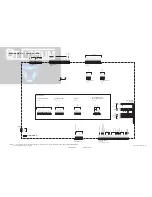
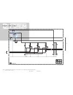
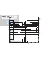
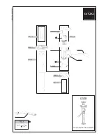
MAIN(MONI) SCHEMATIC DIAGRAM
NOTES: 1. For the destination of each signal and further line connections that are cut off from this diagram, refer to "BOARD INTERCONNECTIONS".
2. The parts with marked ( ) is not used.


