background image

FS-SD550R/FS-SD770R/FS-SD990R

1-9

Prior to performing the following procedure, remove 
the rear cover, the side covers, the front panel 
assembly and the CD mechanism base assembly.

In case that the upper parts of the door arms 
attached to the CD door are not level, let down them 
to the level position by turning the gear a in the 
direction of the arrow.

1.

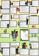
Removing the door arm assembly / the 
door arm board (R) and (L)

(See Fig.15 to 20)

When the door arms incline, the door 
arm assembly and the door arm board 
(R) and (L) may not be removed.

ATTENTION: 

Remove the four screws H  on the upper side and 
the one screw I  on the left side of the body.

Remove the four screws J  attaching the door arm 
board (L) and (R) on both sides of the door arm 
assembly.

2.

3.

Fig.15

Fig.16

Fig.18

Fig.20

Fig.17

Fig.19

Door arm

Door arm board (L)

Door arm

Door arm board (R)

Door arms (Attached to the CD door)

H

H

Door arm assembly

Door arm assembly

J

J

I

Door arm board (L)

Door arm assembly

J

J

Door arm board (R)

Fan motor

Содержание FS-SD550R

Страница 1: ...TE CONTROL DIMMER SLEEP DISPLAY FM MODE AHB PRO CD PROGRAM DOOR SLIDE AUTO PRESET REPEAT RANDOM BASS TREBLE CANCEL UP SET DOWN MD AUX FM AM VOLUME CD FADE MUTING PTY EON DISPLAY MODE FS SD550R FS SD770R FS SD990R REMOTE CONTROL DIMMER SLEEP DISPLAY FM MODE AHB PRO CD PROGRAM DOOR SLIDE AUTO PRESET REPEAT RANDOM BASS TREBLE CANCEL UP SET DOWN MD AUX FM AM VOLUME CD FADE MUTING PTY EON DISPLAY MODE ...

Страница 2: ... Leakage currnet check Electrical shock hazard testing After re assembling the product always perform an isolation check on the exposed metal parts of the product antenna terminals knobs metal cabinet screw heads headphone jack control shafts etc to be sure the product is safe to operate without danger of electrical shock Do not use a line isolation transformer during this check Plug the AC line c...

Страница 3: ...g laserstrålning är denna del är öppnad och spårren är urkopplad Betrakta ej strålen VARO Avattaessa ja suojalukitus ohitettaessa olet alttiina näkymättömälle lasersäteilylle Älä katso säteeseen ADVARSEL Usynlig laserstråling ved åbning når sikkerhedsafbrydere er ude af funktion Undgå udsættelse for stråling ADVARSEL Usynlig laserstråling ved åpning når sikkerhetsbryteren er avslott unngå utsettel...

Страница 4: ...quality during transport and before installation both sides of the laser diode on the replacement optical pickup are shorted After replacement return the shorted parts to their original condition Refer to the text 2 Do not use a tester to check the condition of the laser diode in the optical pickup The tester s internal power source can easily destroy the laser diode 1 2 Handling the traverse unit...

Страница 5: ... laser diode and actuator 2 Do not check the laser diode using a tester as the diode may easily be destroyed 3 It is recommended that you use a grounded soldering iron when shorting or removing the laser diode Recommended soldering iron HAKKO ESD compatible product 4 Solder the land on the optical pickup s flexible cable Note Short the land after shorting the terminal on the flexible cable using a...

Страница 6: ...CD door on the upper side of the body 1 Removing the CD door See Fig 1 Prior to performing the following procedure remove the CD door the rear cover Remove the four screws D attaching the side covers on the bottom of the body Move the left cover backward and remove outward Also remove the right cover in the same way 1 2 Removing the right and left covers See Fig 3 Disassembly method Fig 1 Fig 2 Fi...

Страница 7: ...Disconnect the card wire from connector CN104 and CN105 of the main board in the front part of the body Disconnect the card wire from CN101 of the main board on the right side and the wire from CN705 and CN of the CD mechanism base assembly respectively Remove the four screws F attaching the CD mechanism base assembly on the upper side of the body Remove the screw I attaching the earth terminal on...

Страница 8: ...ed from the door arms pull the CD mechanism base assembly toward the front and disconnect the wire from connector CN804 on the left side of the door arm board Pull out the CD mechanism base assembly toward the front 3 4 5 6 Fig 9 Fig 10 Fig 11 F I CD mechanism base assembly Main board CN101 CN708 F CD mechanism base assembly CN804 CD mechanism base assembly CN301 G Power amplifier board Fig 13 Gea...

Страница 9: ... door arm board R and L See Fig 15 to 20 When the door arms incline the door arm assembly and the door arm board R and L may not be removed ATTENTION Remove the four screws H on the upper side and the one screw I on the left side of the body Remove the four screws J attaching the door arm board L and R on both sides of the door arm assembly 2 3 Fig 15 Fig 16 Fig 18 Fig 20 Fig 17 Fig 19 Door arm Do...

Страница 10: ...rmer assembly 1 2 Removing the transformer assembly See Fig 21 Prior to performing the following procedure remove the CD mechanism base assembly and the door arm assembly Disconnect the wires from connector CN106 on the main board and release it from the cord stopper Remove the three screws N attaching the gear motor assembly Remove the gear motor assembly with the gear motor stopper Remove the be...

Страница 11: ...taching the front panel board inside the front panel assembly 1 Removing the front panel board See Fig 28 Front panel assembly Prior to performing the following procedure remove the CD mechanism base assembly and the door arm assembly To facilitate operation process remove the gear motor assembly before performing the following procedure Disconnect the wires from connector CN102 CN106 CN191 CN192 ...

Страница 12: ...ly and disconnect the wire from connector CN703 and CN706 on the CD mechanism board Turn over the CD mechanism base assembly and disconnect the wires from connector CN703 and CN706 on the CD mechanism board Turn back the CD mechanism assembly and detach the CD mechanism cover while pulling the CD mechanism assembly outward to release the two joint tabs marked c 1 2 3 Removing the CD mechanism boar...

Страница 13: ...assembly from the three shafts of the CD mechanism cover 4 5 6 When reassembling confirm that the cushion of the CD mechanism assembly is reattached to the three shafts ATTENTION Remove the CD mechanism board from the CD mechanism cover 7 Fig 33 Fig 32 CD mechanism assembly CD mechanism cover CD mechanism board CN605 Cushion Cushion CD mechanism cover CD mechanism board Shafts Short circuit land S...

Страница 14: ...wire from connector CN502 on the jack board Remove the six screws W attaching the switch board 1 2 Removing the switch board See Fig 35 Disconnect the harness from connector CN706 on the CD mechanism board on the underside of the CD mechanism base assembly Push inward the two tabs d attaching the LED board case and release them Pull out the LED board from the LED board case 1 2 3 Removing the LED ...

Страница 15: ...hen the life of the laser diode has expired the following symptoms will appear 1 The level of RF output EFM output amplitude of eye pattern will below Is the level of RFOUT under 1 25V 0 22Vp p Replace it NO YES O K 3 Semi fixed resistor on the APC PC board The semi fixed resistor on the APC printed circuit board which is attached to the pickup is used to adjust the laser power Since this adjustme...

Страница 16: ... finishes Automatic measurement of TE amplitude and automatic tuning of TE balance 500mv div 2ms div Fig 1 Approx 3sec pin 25 of IC601 TE Approx 1 8V VREF Tracking error waveform at TOC reading Power ON Play Key Confirm that the Focus error S cuve signal at the pin28 of IC603 is approx 2Vp p Confirm that the signal from pin24 IC603 is 0V as a accelerated pulse during approx 400ms Confirm the wavef...

Страница 17: ...it before removing the pickup Then carry out the replacement Refer to Dismantling and assembling the traverse unit on page 1 5 When the KSM 900AAH mechanism is used the expansion cable is used as follows EXTFSSD5 JIG extension wire QUQB12 0840CJ 8pin card wire QUQB12 0940DJ 9pin card wire QUQB12 1840DJ 18pin card wire QUQB12 1640DJ 16pin card wire EXTKSM900 JIG Sub board ...

Страница 18: ...ASS22 OUT1 BASS11 BASS12 MID11 MID12 MID21 MID22 TRE2 TRE1 VOL1 VOL2 GOUT2 GOUT1 CH1 input pin A CH2 input pin A CH1 input pin B CH2 input pin B CH1 input pin C CH2 input pin C CH1 input pin D CH2 input pin D CH1 input pin E CH2 input pin E Microphone input pin Filter pin Ground pin Serial data latch receiving pin Serial clock receiving pin Power supply pin CH2 output pin CH2 bass filter setting p...

Страница 19: ...lifier outputs ON OFF BTL AMP 1 input pin BTL AMP 1 input pin For gain adjustment BTL AMP 1 input pin Non inverting side BTL AMP 1 input pin Inverting side BTL AMP 2 input pin Inverting side BTL AMP 2 input pin Non inverting side BTL AMP 2 input pin For gain adjustment BTL AMP 2 input pin External transistor collector PNP connection 5V power supply output External transistor PNP base connection Re...

Страница 20: ...TE RAM 1024 BYTE 16 bit TIMER EVENT COUNTER 8 bit TIMER EVENT COUNTER50 PORT0 PORT1 PORT2 PORT3 PORT4 PORT5 PORT6 PORT7 EXTERNAL ACCESS SYSTEM CONTROL 8 bit TIMER EVENT COUNTER51 SERIAL INTERFACE30 SERIAL INTERFACE31 UART0 INTERRUPT CONTROL A D CONVERTER VDD0 VDD1 Vss0 Vss1 IC BUZZER OUTPUT CLOCK OUTPUT CONTROL WATCHDOG TIMER WATCH TIMER ...

Страница 21: ...ltage detection for safety CD door motor lock detection signal input Version detection Reference voltage input for A D converter Analog power supply for A D converter System reset signal input Sub clock Sub clock signal input 32 768kHz Connect to VSS0 or VSS1 Main clock Main clock signal input 4 19MHz Ground without port section Remote controller signal input RDS clock signal input Sub clock OSC c...

Страница 22: ...SEL MLD MCLK MDATA DSL PLL VCO AVDD2 SUB CODE BUFFER SSEL SQCK SUBQ AVDD2 CLVS CRC BLKCK CLDCK SBCK SUBC DEMPH RESY FLAG6 RESY EFM DEMODULATION SUBCODE DEMODULATION SYNC INTERPOLATION 16k SRAM CIRC ERROR CORRECTION DEINTERLEVE LRCKIN MSEL BCLK SSEL SRDATAIN PSEL IOSEL DIGITAL DEEMPHSIS 8TIMES OVER SAMPUNC DIGITAL FILTER 1BIT DAC LOGIC S PEM R PEM L DIGITAL AUDIO INTERFASE DIGITAL AUDIO INTERFASE I...

Страница 23: ...ck pulse output Tracking drive output Focus drive output Reference voltage input pin for D A output block TVD FOD FBA TBAL Focus Balance adjust signal output Tracking Balance adjust signal output Focus error signal input Analog input Tracking error signal input Analog input RF envelope signal input Analog input Vibration detect signal input H detect Off track signal input H off track Track cross s...

Страница 24: ...ground shorting protection circuit Overvoltage thermal protection circuit Input amplifier BEEP amplifier Input amplifier A B D C Nonlinear output stage Amplifier output stage SW drive A B C D H L S STBY D C PRE GND IN 1 IN 2 ON TIME BEEP Vcc Vcc SW SW B SW E SW OUT1 SW OUT2 SW GND OUT 1 OUT 2 N C OUT 1 OUT 2 PWR GND 1 PWR GND 2 H L S Higher Level signal selector Ripple filter LA4905 IC301 2ch BTL ...

Страница 25: ... TEBPF TEOUT TEN FEN FEOUT GCTL FBAL TBAL E F D B C A Earth terminal VREF output terminal VDET output terminal VDET input terminal TE Amp output terminal TE Amp reversing input terminal FE Amp reversing input terminal FE Amp output terminal Terminal GCTL APC FBAL control terminal TBAL control terminal Tracking signal input terminal 1 Tracking signal input terminal 2 Focus signal input terminal 4 F...

Страница 26: ... GND CIN OUT Pin No Symbol I O QUAL DA O VREF O MUX I VDD GND CIN I OUT O GND 10 GND 11 GND 12 VDD 13 XI I 14 XO O 15 TS7 16 CL O Function Non connection RDS data output Reference voltage output Multiplex signal input 5Vsupply voltage for analog Ground for analog part 0V Sub carrier output of reconstruction filter Ground for digital part 0V Ground for digital part 0V Ground for digital part 0V Gro...

Страница 27: ...CIRCUIT Vcc 2 2 9 10 1 1 IN1 IN2 STANDBY CIRCUIT THERMAL SHUTDOWN CIRCUIT TA8409F W IC108 Bridge driver 1 Pin layout 2 Pin function 3 Block diagram 1 5 10 6 1 2 3 4 5 6 7 8 9 10 INput terminal Supply voltage terminal for logic Output terminal Non connection GND terminal Non connection Supply voltage terminal for motor driver Output terminal Reference voltage terminal for control circuit Input term...

Страница 28: ...er on reset Input output port Input output port Data input output Function IF counter signal input IF signal output Not use AM Local OSC signal output FM Local OSC signal input Power suplly VDD 4 5 5 5V When power ON Reset circuit move PLL charge pump output H Local OSC frequency Height than Reference frequency L Low Agreement Height impedance Input for active lowpassfilter of PLL Output for activ...

Страница 29: ...ch Output Lch Voltage controlled terminal When voltage of terminal is MONO at H and ST at L When voltage of terminal is AM at H and FM at L Multi plex signal input AM detection signal output FM detection signal output Bypass to FMIF Input of AMIF signal Fixed voltage output terminal Output terminal for AM mixer Input of FMIF signal Function Function 2 Pin Function 1 Block Diagrams 24 23 22 21 20 1...

Страница 30: ... IN 5 B IN A B NJM4580D D IC101 Dual ope amp 1 Pin layout Block diagram GP1U271X IC801 Receiver for remote GND B P F VCC Vout Amp Limiter Integrator Comparator Demodulator 1 Pin layout 2 Block diagram INPUT D2 Q12 Q14 R12 R10 R11 R13 R14 Q13 R4 OUTPUT R7 Q7 GND Q1 Q6 Q4 Q11 Q2 Q3 R5 R6 R4 R1 R2 R3 C1 Q5 Q8 Q9 R17 R9 R13 Q10 R14 R15 D1 R16 Q15 OUTPUT INPUT GND UPC78L05J T IC191 Regulator ...

Страница 31: ...pan 200103 V VICTOR COMPANY OF JAPAN LIMITED AUDIO COMMUNICATION BUSINESS DIVISION PERSONAL MOBILE NETWORK BUSINESS UNIT 10 1 1Chome Ohwatari machi Maebashi city 371 8543 Japan No 20923 FS SD550R FS SD770R FS SD990R ...

Отзывы: