


1-34
FS-A52
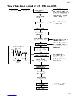
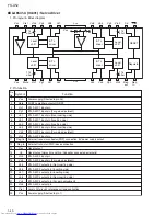
UPD780024AGKB21 (IC251) : Unit micon
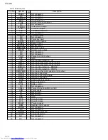
1. Pin layout
2. Pin function (1/2)
1
~
16
48
~
33
17 ~ 32
64 ~ 49
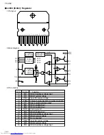
1
2
3
4
5
6
7
8
9
10
11
12
13
14
15
16
17
18
19
20
21
22
23
24
25
26
27
28
29
30
31
32
Pin
No.
Symbol
I/O
Description
P50/A8
P59/A9
MCS
MRDY
CDINDEX
CDEMP
CDTNO
CDCOPY
VSS0
VDD0
P30
P31
P32
MUTE
SUBQ
P35/SO31
SQCK
KCMND
MSTAT
MCLK
RXDO
TXDO
P25/SCK0
VDD1
AVSS
KEY1
KEY2
PCHK
P14/AN14
P13/AN13
/OPEN
/REST
-
-
-
-
-
I
I
I
-
-
-
-
-
O
I
-
O
O
O
I
I
O
-
-
-
I
I
I
-
-
I
I
Connected to GND
Not used
Pull-up +B
Not used
Not used
CD emphasis detection
CD track No. detection
CD copy detection
GND
Power supply
Not used
Not used
Not used
Mute output
Sub-code Q data input from IC651
Not used
Sub-code Q register clock output to IC651
Kick command data
CD control status output to IC801
CD control command clock input from IC801
Digital data input
Digital data output
Connected to GND
Power supply
GND
Key input 1
Key input 2
Parity check
Connected to GND
Connected to GND
Open switch input
Rest switch input
Содержание FS-A52
Страница 49: ...1 49 FS A52 M E M O ...
Страница 52: ...FS A52 3 2 M E M O ...
Страница 69: ...FS A52 3 19 M E M O ...
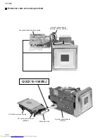
Страница 78: ...A B C D E F G 1 2 3 4 5 2 7 FS A52 Main board Printed circuit boards ...
Страница 79: ...FS A52 FS A52 A B C D E F G 1 2 3 4 5 2 8 Power amplifier board ...
Страница 81: ...A B C 1 2 3 4 5 FS A52 2 10 Tuner board ...


