background image

MX-K1

1-17

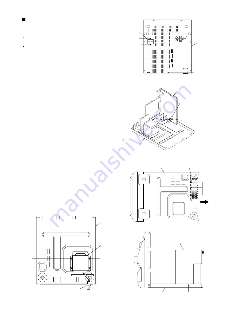
Fig.34

  Prior to performing the following procedures, 

remove the top cover.
Also remove the CD changer unit.

1.

2.

3.

4.

5.

6.

7.

8.

Remove the two screws "X" that retain the 
SPEAKERS terminals.
Remove the screw "Y" that retains the rear panel, 
and then remove the rear panel.
Disconnect the parallel wires from the connectors 
CN901A and CN901B on the power amp and 
supply PCB.
Disconnect the parallel wire and card wire from 
the connectors CN101 and CN901 on the power 
amp and supply PCB.
Remove the three screws "Z" retaining the heat 
sink onto the bottom of the chassis.
Remove the screw "AA" that retain the power amp 
and supply PCB and then remove the assembly.
Remove the clamp of AC power cord from the 
chassis.
Remove the four screws "AB" that retain the 
power trans PCB and then remove the assembly.

Removing the power amp and supply 
PCB and the power trans PCB

 (See Fig.33 to 37)

Fig.36

Fig.35

(Top view)

Fig.37

Fig.33

Rear panel

Speaker
terminal

Y

X

Chassis

Chassis

AA

Power amp and
       supply PCB

Heat sink

Rear

Z

Chassis

Power amp and
       supply PCB

CN901B

CN901A

AB

Chassis

Power trans PCB

Clamp

AC power cord

AB

Содержание CA-MXK1

Страница 1: ... ON STANDBY PHONES REPEAT PROGRAM RANDOM STOP REC START DUBBING REC START CD CLOCK TIMER TAPE A B DISC SKIP EJECT PLAY A REC PLAY B CD CONTROL CD 1 A U X F M A M C D T A P E CD 2 CD 3 CD R RW PLAYBACK VCD NUMBER RETURN PBC MAX MIN MIC MIC VOL CANCEL SET 1 BIT DUAL D A CONVERTER PRESET TUNNIG DEMO COMPU PLAY CONTROL ACTIVE BASS EXTENSION FULL LOGIC CONTROL CD SYNCHRO RECORDING EJECT R O C K CLASSIC...

Страница 2: ...et screw heads headphone jack control shafts etc to be sure the product is safe to operate without danger of electrical shock Do not use a line isolation transformer during this check Plug the AC line cord directly into the AC outlet Using a Leakage Current Tester measure the leakage current from each exposed metal parts of the cabinet particularly any exposed metal part having a return path to th...

Страница 3: ...laserstrålning är denna del är öppnad och spårren är urkopplad Betrakta ej strålen VARO Avattaessa ja suojalukitus ohitettaessa olet alttiina näkymättömälle lasersäteilylle Älä katso säteeseen ADVARSEL Usynlig laserstråling ved åbning når sikkerhedsafbrydere er ude af funktion Undgå udsættelse for stråling ADVARSEL Usynlig laserstråling ved åpning når sikkerhetsbryteren er avslott unngå utsettelse...

Страница 4: ...optical pickup The tester s internal power source can easily destroy the laser diode 4 Handling the CD changer unit optical pickup 1 Do not subject the CD changer unit optical pickup to strong shocks as it is a sensitive complex unit 2 Cut off the shorted part of the flexible cable using nippers etc after replacing the optical pickup For specific details refer to the replacement procedure in the t...

Страница 5: ...ette deck mechanism Removing the earphone jack PCB Removing the control FL PCB Removing the switch PCB and ACTIVE BASS EX switch PCB Removing the cassette deck main motor and replacing the main belts Removing the leaf switches of the cassette deck mechanism Removing the cassette deck heads Chassis unit Removing the 3 pin regulator Removing the power amp and supply PCB and the Power Trans PCB Comme...

Страница 6: ...ve the top cover Also remove the rear panel See Fig 33 Remove the screw A from the bracket that retains the power IC Remove the solder fixing the power IC Replacing the power IC See Fig 2 and 3 Fig 3 Fig 2 Disassembly of the main blocks of this set Replacement of the fuses and the power IC A Heat sink Power amp and supply PCB Fuse F951 1A 250V Power trans PCB Fuse F952 1 6A 250V Chassis Power amp ...

Страница 7: ...move the six screws B that retain the top cover from the rear of the body Remove the four screws C that retain the top cover from the two sides of the body Remove the top cover from the body by lifting it toward the rear Fig 5 B B B Top cover Front panel assembly C ...

Страница 8: ...onnectors CN307 and CN308 on the main PCB which is located below the CD changer unit Disconnect the card wires from the connectors CN301 CN302 and CN305 on the main PCB Disconnect the parallel wires from the connectors CN902A CN902B and CN902C on the power amp and supply PCB From the rear of the set remove the two screws D retaining the CD changer unit then remove the three screws E and the screw ...

Страница 9: ...the front panel assembly onto the bottom of the body Remove the screw H retaining the cassette deck mechanism and then remove the GND lug b that comes from the power amp and supply PCB Remove the solder connecting the wire on the control FL PCB Disengage the claws c on both sides at the bottom of the front panel assembly and then remove the assembly Removing the front panel assembly See Fig 10 and...

Страница 10: ...the screw with the washer J that retain the main PCB should be removed Remove the main PCB by pulling it toward the side where the CN601 is located Using solder short the CD pickup to connect to short round Disconnect the card wire from the connector CN601 on the main PCB and then remove the main PCB Removing the main PCB See Fig 12 and 13 Fig 13 Disassembly of units and assembly inside this set C...

Страница 11: ...sm assembly Remove the two screws K retaining the CD changer mechanism assembly Removing the CD changer mechanism assembly See Fig 14 to 16 Fig 16 Fig 15 Caution When replacing the CD changer mechanism assembly be sure not to mistake the positions of the red and blue dampers Note When re assembling after the disassembly work apply bonding agent on the spring to prevent it from slipping off Spring ...

Страница 12: ... unit 1 2 3 4 5 6 Remove the two screws M retaining the stopper brackets on both sides of the CD changer unit Remove the stopper brackets from both sides of the CD changer unit Pull out the CD tray from the CD changer unit all the way and then lift the tray upward to remove Turn the CD tray upside down and remove the tray rotor belt from the pulley Turn the CD tray upside down and disconnect the c...

Страница 13: ...e the CD changer unit Also remove the front panel assembly 1 Remove the screw with the washer P that retains the earphone jack PCB from the back of the front panel assembly Removing the earphone jack PCB See Fig 22 Prior to performing the following procedure remove the top cover Also remove the CD changer unit 1 Remove the three screws Q that retain the control FL PCB from the back of the front pa...

Страница 14: ...ining the volume knob shaft Remove the three screws Q retaining the control FL PCB from the back of the front panel assembly Remove the control FL PCB Remove the eleven screws R retaining the switch PCB Remove the two screws S retaining the ACTIVE BASS EX switch PCB Removing the switch PCB and ACTIVE BASS EX switch PCB See Fig 23 to 26 Fig 25 Fig 26 R R S ACTIVE BASS EX switch PCB Switch PCB Volum...

Страница 15: ...gths of the cassette A playback only and cassette B record play main belts are different When attaching the main belts use the longer belt for cassette A Prior to performing the following procedures remove the top cover Also remove the CD changer unit Also remove the front panel assembly 1 2 3 4 5 Remove the five screws O that retain the cassette deck mechanism Remove the cassette deck mechanism T...

Страница 16: ...he head Loosen the screw V that retains the head Hold the head and slide it in the direction of the arrow to remove it Removing the cassette deck heads See Fig 21 and 30 Fig 31 Fig 32 Prior to performing the following procedures remove the top cover Also remove the rear panel See Fig 33 1 2 Remove the screw W that retains the bracket holding the 3 pin terminal regulator Remove the solder fixing th...

Страница 17: ...1 on the power amp and supply PCB Remove the three screws Z retaining the heat sink onto the bottom of the chassis Remove the screw AA that retain the power amp and supply PCB and then remove the assembly Remove the clamp of AC power cord from the chassis Remove the four screws AB that retain the power trans PCB and then remove the assembly Removing the power amp and supply PCB and the power trans...

Страница 18: ...quency Range AM 531kHz 1710kHz FM 87 5MHz 108MHz Standard measurement positions of volume and switch Power Standby Light STANDBY Indicator S A BASS OFF Sound mode OFF Main VOL 0 Minimum Travers mecha set position Disc 1 Mic MIX VOL MAX ECHO OFF Precautions for measurement 1 Apply 30pF and 33kohm to the IF sweeper output side and 0 082 F and 100kohm in series to the sweeper input side 2 The IF swee...

Страница 19: ...il L301 Use the High Impedance Probe for Frequency counter input Cassette Head Azimuth Alignments Recording Bias Frequency Alignment Items Measurement conditions Measurement method Standard values Adjusting positions OSC coil adjustment 1 Set the Signal Generator signal to 530KHz the feed to Loop Antenna 2 Receiving the signal and the adjust the OSC coil L2 obtain the V T is 1 40V 0 05V Antenna co...

Страница 20: ...Automatic measurement of TE amplitude and automatic tuning of TE balance 500mv div 2ms div Fig 1 Approx 3sec pin 20 of IC611 TE Approx 1 8V VREF Tracking error waveform at TOC reading Power ON Play Key Confirm that the Focus error S cuve signal at the pin32 of IC601 is approx 2Vp p Confirm that the signal from pin24 IC601 is 0V as a accelerated pulse during approx 400ms Confirm the waveform of the...

Страница 21: ... of the laser diode has expired the following symptoms will appear 1 The level of RF output EFM output ampli tude of eye pattern will below Is the level of RFOUT under 1 25V 0 22Vp p Replace it NO YES O K 3 Semi fixed resistor on the APC PC board The semi fixed resistor on the APC printed circuit board which is attached to the pickup is used to adjust the laser power Since this adjustment should b...

Страница 22: ...necting terminal for HPF Amp 10 3TOUT O 3 TENV output terminal 11 CBOO I Capacitor connecting terminal for envelope detection on the darkness side 12 BDO O BDO output terminal 13 COFTR I Capacitor connecting terminal for envelope detection on the light side 14 OFTR O OFTR output terminal 15 NRFDET O NRFDET output terminal 16 GND Ground 17 VREF O VREF output terminal 18 VDET O VDET output terminal ...

Страница 23: ...OUT2 O CH2 positive output 5 IN2 I CH2 input 6 IN1 I CH1 input 7 VCC Power supply terminal 8 VCC Power supply terminal 9 REG I I Regulator current detection terminal 10 REG B O Connect to base terminal of external transistor 11 REG OUT O Constant voltage output Connect to collector terminal of external transistor 12 IN3 R I CH3 reverse input 13 IN3 F I CH3 forward input 14 OUT3 O CH3 positive outp...

Страница 24: ...oltage input terminal 13 FM_DET O FM detection signal output 14 ST MON_SW I Stereo Monaural switching signal input 15 AM FM_SW I AM FM switching signal input 16 L_OUT O Output L channel 17 R_OUT O Output R channel 18 MPX_IN I Multiplex signal input 19 DET_OUT O AM FM detection output 20 FM_OSC FM local oscillation circuit 21 VCC_2 Power supply terminal 22 FM_RFOUT O Output of FMRF signal 23 GND_2 ...

Страница 25: ... Open state after the power on reset Input output port Input output port Data input output Function IF counter signal input IF signal output Not use AM Local OSC signal output FM Local OSC signal input Power supply VDD 4 5 5 5V When power ON Reset circuit move PLL charge pump output H Local OSC frequency Height than Reference frequency L Low Agreement Height impedance Output for active lowpassfilt...

Страница 26: ...nal for recording amp 16 REC_OUT2 O Output for recording amp 17 CG O Charge detection terminal 18 VCC Power supply terminal 19 A B_SW I REC amp Select switch A cassette B cassette 20 PREOUT2 O Output terminal for playback amp 21 EQ2 O Metal output for playback amp 22 NF2 I NF terminal for playback amp 23 CH2_B I Input for playback amp Ch2 B cassette REC PB 24 CH2_A I Input for playback amp Ch2 A c...

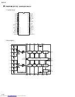
Страница 27: ...CC OE Q5 Q6 Q7 Q8 Q S QS Ø Ø Ø Ø Ø Ø ØS D LATCH F F 2 SI D Q Q 3 CK Ø Ø 1 ST 15 OE Q ØS Q D Ø Ø F F ØS ØS D Q ØS ØS LATCH 4 Q1 5 Q2 D Q Q Ø Ø F F D Q ØS ØS LATCH 6 Q3 D Q Q Ø Ø F F D Q ØS ØS LATCH 7 Q4 D Q Q Ø Ø F F D Q ØS ØS LATCH 14 Q5 D Q Q Ø Ø F F D Q ØS ØS LATCH 13 Q6 D Q Q Ø Ø F F D Q ØS ØS LATCH 12 Q7 D Q Q Ø Ø Ø Ø F F D Q ØS ØS LATCH 11 Q8 QS 9 Q S 10 ...

Страница 28: ...UT MULTIPLEXER GAIN BASS BIN L BASS SPKR ATT RIGHT BOUT R BIN R SUPPLY CREF AGND VS 27 4 5 6 7 3 2 1 28 21 22 20 26 24 25 10 11 19 12 13 23 8 9 18 14 15 RB RB VREF 2 Block diagram LIN3 LIN4 MUXO L IN L MUXO R BIN R IN R BOUT R BIN L 1 3 2 4 5 6 7 8 9 BOUT L N C N C TRE R TRE L SCL SDA DGND CREF 23 22 21 20 19 17 18 16 15 10 11 12 13 14 28 27 26 25 24 RIN3 RIN2 RIN1 LIN1 LIN2 VS AGND ROUT LOUT RIN4...

Страница 29: ...rive signal Servo error signal output Kick pulse output Tracking drive output Focus drive output Reference voltage for D A output block Focus balance adjust signal output Tracking balance adjust signal output Focus error signal input Analog input Tracking error signal input Analog input RF envelope signal input Analog input Vibration detect signal input H Detect Off track signal input H Off track ...

Страница 30: ...3 12 11 10 9 8 7 6 5 4 3 2 1 VSS OUT OUTPUT VDD OUT N C N C MUTE STAND BY VSS PRE VDD PRE BOOST N C IN MUTE IN IN STAND BY GND Top view BOOST OUTPUT VDD PRE VSS PRE IN IN BOOTSTRAP BIPOLAR TRANSCONDUCTANCE INPUT STAGE MDS GAIN LEVEL SHIFTING STAGE MOS OUTPUT STAGE SHORT CIRCUIT PROTECTION ...

Страница 31: ...Printed in Japan 200105 S No 20942 MX K1 VICTOR COMPANY OF JAPAN LIMITED AUDIO COMMUNICATION BUSINESS DIVISION PERSONAL MOBILE NETWORK B U 10 1 1Chome Ohwatari machi maebashi city 371 8543 Japan ...

Страница 32: ...et screw heads headphone jack control shafts etc to be sure the product is safe to operate without danger of electrical shock Do not use a line isolation transformer during this check Plug the AC line cord directly into the AC outlet Using a Leakage Current Tester measure the leakage current from each exposed metal parts of the cabinet particularly any exposed metal part having a return path to th...

Страница 33: ...le pos P C B Ass y Turn Table motor Parallel wire Tray SW P C B Ass y Disc count P C B Ass y Pick up SW P C B Ass y Active bass EX Switch P C B Ass y W603 W606 Switch P C B Ass y Control FL P C B Ass y FL TUBE Power trans P C B Ass y Head phone P C B Ass y Parallel wire Card wire Parallel wire Card wire Card wire CN901 1 CN603 Color codes are shown below 1 Brown 2 Red 3 Orange 4 Yellow 5 Green 6 B...

Страница 34: ...702 FL display CN101 CN901 CN701 VCK VDATA SCK SDI SDO TUCE Block diagram AUX IN JA301 ANT TERMINAL JA302 A cassette B cassette Q403 Q404 Q503 Q504 16 9 REC L REC R CH2_B CH1_B REC_OUT2 REC_OUT1 CH2_A CH1_A PREOUT2 PREOUT1 20 5 REC_IN2 REC_IN1 14 11 A B RPHD 19 19 A B_SW SOLA SOLB MOT DM DM TM TM T T F F DCNT TPSW UPSW DWSW CLSW OPSW CW CCW CNTT ARF RFENV BDO OFT RFDET FOD TRD KICK TRV TVD ECM ECS...

Страница 35: ...K R509 150K R409 150K C510 0 0033 C410 0 0033 C511 25V10 C411 25V10 C306 10V47 R306 1M R512 1 8K R513 22K R514 4 7K R413 22K R414 4 7K R412 1 8K C515 25V4 7 C415 25V4 7 Q501 2SD2144S Q401 2SD2144S C514 1000P C414 1000P PB HD RP HD C508 25V4 7 C408 25V4 7 R505 10K R405 10K C509 1000P C409 1000P C517 470P C417 470P R415 10K R515 10K L301 BIAS COIL C308 0 015 M Q303 KTC3203Y R308 10K R311 12 C311 0 0...

Страница 36: ... 33K C649 50V10 R666 1K R665 18K R662 5 6K R663 5 6K R664 18K Q602 DTC114YS R670 390K R671 8 2K C603 0 0022 R604 1K C602 0 0022 R603 1K OPSW CLSW UPSW DWSW DCNT TPSW OPN CLS CCW CW CNTT MLD REST XRST MOMU STAT MCLK MDATA SQCK SUBQ OUT R A GND OUT L M 8V D GND CD 5V M GND C604 2200P SW5V CCW CW CNTT OPN CLS CCW CW CNTT UPSW DWSW CLSW OPSW OPSW CLSW UPSW DWSW DCNT TPSW DCNT TPSW SQCK SUBQ MLD XRST M...

Страница 37: ...6 7 8 9 10 FW701 1 2 3 4 5 6 7 8 9 10 FW701 R1064 12K SMUTE PCNT SPK PRT INH SFTY ACSW FTU LVL MPX AHB SDO SDI SCK TUCE XRST FCD REST MOMU MLD SUBQ SQCK VCK VDAT RDCK RDDI OPSW CLSW UPSW DWSW DCNT TPSW OPN CLS CCW CW CNTT RECM PBM TPA TPB EXCE MCLK MDATA KOK ECHO AHB RECM PBM KOK ECHO OPN CLS CW CCW CNTT OPSW CLSW UPSW DWSW DCNT TPSW REST PCNT FTU FCD SPK SUBQ SQCK SDO SDI SCK TPA TPB LVL SFTY ACS...

Страница 38: ...7K R227 1 2K R223 56K C217 100P C219 27P C216 100P C222 0 1 M C223 0 1 M C221 50V22 C218 50V47 C323 50V10 D301 1N4002 Q205 R222 4 7K R135 R235 R236 R136 Q105 R237 R137 Q204 KTC3199 Q104 KTC3199 R122 4 7K R327 EP901 R120 3 3K R220 3 3K R133 R233 R319 R321 R320 R323 R322 C326 C327 Q308 Q309 Q307 D310 D201 NOMT D101 NOMT C325 R318 R325 CJ9029 18 0200A R132 0 R232 0 0V 0V 0V 0V 0V 16 87V 34 3V 34 3V 8...

Страница 39: ... assurance parts When replacing those parts make sure to use the specified one F951 1A 250V F952 1 6A 250v 1 2 3 4 5 6 7 8 9 FW951 AC PLUG R951 3 3M 1 2W J C Version 120V 60Hz 11 5 13 14 15 8 10 2 9 12 16 6 T951 EI 66 Power transformer section To I 3 on page 2 8 ...

Страница 40: ...6 5 4 3 2 1 B C D E F G H I J A 7 MX K1 2 10 MX K1 Main circuit board TRAY SW PCB PICK UP SW PCB TURN TABLE MOTOR PCB MAIN PCB DISC COUNT PCB TABLE POS PCB Printed circuit boards ...

Страница 41: ...6 5 4 3 2 1 B C D E F G H I J A 7 MX K1 2 11 Control FL and Switch circuit board ACTIVE BASS EX SWITCH PCB CONTROL FL PCB HEAD PHONE PCB SWITCH PCB ...

Страница 42: ...6 5 4 3 2 1 B C D E F G H I J A 7 MX K1 2 12 MX K1 Power amp and Power supply circuit board ...

Страница 43: ...MX K1 2 3 6 5 4 3 2 1 B C D E A 7 Power trans circuit board 2 13 ...

Страница 44: ...MX K1 2 4 MEMO 2 14 ...

Страница 45: ...MX K1 2 5 2 15 MEMO ...

Страница 46: ...able as service parts Contents Exploded view of general assembly and parts list Cassette mechanism assembly and parts list CD mechanism assembly and parts list Electrical parts list Packing materials and accessories parts list MX K1 3 2 3 5 3 6 3 9 3 19 Area suffix J U S A C Canada ...

Страница 47: ...MX K1 3 2 A B C 1 2 3 4 5 Exploded view of general assembly and parts list Block No M M M 1 54 ...

Страница 48: ...19A ASS 22 GJ560530200101 BOTTOM CASE 1 23 GJ4B05315001E0 CD FITTING 1 24 GJ727450540503 SOLDER TAG 1 25 GJ336660190013 POWER TRANS A 1 AC120V 60HZT951 26 AC POWER PCB 1 ASS Y 27 GJ780000180100 HEAT SINK 1 28 POWER AMP PCB 1 29 GJ560170100101 BRACKET A 1 30 GJ560170110101 BRACKET B 1 31 GJ780000340100 HEAT SINK 1 32 MAIN PCB 1 33 GJ560170040101 PCB BRACKET 1 34 CD CHANGER UNIT 1 910 EXLM75 03 35 G...

Страница 49: ...ption Block No M1MM 49 GJ703260800100 SPECIAL SCREW 1 TT 2 6X8 D10 B 50 GJ702264400610 SCREW 4 TT 4X6 PW 8 TY 51 GJ703300802000 SCREW 1 TT3X8 D 12 BW 52 GJ702244301050 SCREW 2 TT 3X10 BV TYP 53 GJ735000040003 INSULATOR 1 54 GJ350162001119 POWER CORD A 1 General aasembly ...

Страница 50: ...No CMAT6Z216A or CMAT6Z219A for Cassette Mechanism Assembly Unit L SIDE TYPE R SIDE TYPE Item Parts number Parts name Area A Parts list Cassette mechanism Q ty Description Block No M2MM 1 F513 858 PLATE HD BLK 1 2 F525 338 MTR MAIN BLK 1 3A PCB CONTROL BLK 1 CMAT6Z216A 3B PCB CONTROL BLK 1 CMAT6Z219A 4 UE20P 12 LEAF SWITCH 5 CMAT6Z216A UE20P 12 LEAF SWITCH 3 CMAT6Z219A 5 F522 063 CLUTCH ASSY BLK 2...

Страница 51: ...k No M M M 3 20 20 20 40 62 61 35 57 55 54 34 47 49 19 19 19 19 62 66 62 67 59 58 46 46 45 48 48 44 44 16 63 64 38 37 39 56 65 14 19 18 62 42 26 23 22 6 3 33 14 14 13 12 33 33 36 32 30 31 4 10 5 7 8 9 59 58 21 1 60 11 15 43 43 24 27 25 17 41 50 52 51 29 2 2 28 ...

Страница 52: ...1 GJ4A04300101A1 TURRETTO 1 22 GJ700263261042 SCREW 1 2 6 X 10 BLACK 23 GJ560430050101 BLIND SHEET 1 24 GJ729421400300 WASHER 1 4 X 14 X 0 3T 25 GJ711001620100 SPRING 1 CHANGER GEAR 26 GJ4D04300701A1 CHANGER GEAR 1 27 GJ721311000500 WASHER 1 3 1 X 10 X 0 5T 28 GJ4B04301201A2 MAINCHASSIS 1 29 GJ381020310004 MOTOR 2 TRAY MOTOR 30 GJ4L04301901A1 SLIDE GEAR 1 31 GJ4D04300401A1 GEAR PULLEY A 1 32 GJ560...

Страница 53: ...SWITCH PWB 1 TURN TABLE 55 SWITCH PWB 1 TRAY SWITCH 56 SWITCH PWB 1 DISC COUNT 57 SWITCH PWB 1 PICK UP 58 GJ302237001 RUBBER CUSHION 1 59 GJ302237011 RUBBER CUSHION 1 60 GJ4O04302101A1 MECHA BASE 1 61 GJ390170021204 SWITCH DIRECT 1 62 GJ700264261840 SCREW 1 63 GJ711001650100 SPRING 1 64 GJ711001660100 SPRING 1 65 GJ560533800101 SHIELD RING 1 66 EXL M71 03 CD MECHA UNIT 1 67 OPTIMA 7B PICK UP ASS Y...

Страница 54: ...PACITOR 25V VX M 4 7UF C 107 GJ270144750310 E CAPACITOR 25V VX M 4 7UF C 108 GJ270144750310 E CAPACITOR 25V VX M 4 7UF C 109 GJ270144750310 E CAPACITOR 25V VX M 4 7UF C 110 GJ283108232415 P CAPACITOR 50V K 0 082UF C 111 GJ283108232415 P CAPACITOR 50V K 0 082UF C 112 GJ283105622415 P CAPACITOR 50V K 0 0056U C 113 GJ283101242415 P CAPACITOR 50V K 0 12UF C 114 GJ283101042415 P CAPACITOR 50V K 0 1UF C...

Страница 55: ...PACITOR 50V B K 330PF C 626 GJ116259621 C CAPACITOR 25V F Z 0 022UF C 627 GJ116221121 C CAPACITOR 50V SL J 33PF C 628 GJ283112732432 P CAPACITOR 100V K 0 027UF C 629 GJ111067121 C CAPACITOR 47000PF F Z 50V C 630 GJ116230221 C CAPACITOR 16V X M 0 0022U C 631 GJ270112270310 E CAPACITOR 10V VX M 220UF C 632 GJ283112732432 P CAPACITOR 100V K 0 027UF C 633 GJ282031032415 M CAPACITOR 50V J 0 01UF C 635 ...

Страница 56: ...312030111210 TRANSISTOR KTC3199TPGR Q 319 GJ312011231210 TRANSISTOR KTA1267Y Q 321 GJ872990437 TRANSISTOR DTC114YS Q 401 GJ872992241 TRANSISTOR 2SD2144STPUVW Q 402 GJ872992241 TRANSISTOR 2SD2144STPUVW Q 501 GJ872992241 TRANSISTOR 2SD2144STPUVW Q 502 GJ872992241 TRANSISTOR 2SD2144STPUVW Q 601 GJ312011231210 TRANSISTOR KTA1267Y Q 602 GJ872990437 TRANSISTOR DTC114YS R 1 GJ250031522199 CARBON RESISTOR...

Страница 57: ...SISTOR 1 4WM J 1K R 339 GJ250032222199 CARBON RESISTOR 1 4WM J 2 2K R 340 GJ250032222199 CARBON RESISTOR 1 4WM J 2 2K R 341 GJ250032222199 CARBON RESISTOR 1 4WM J 2 2K R 344 GJ250031022199 CARBON RESISTOR 1 4WM J 1K R 345 GJ250031022199 CARBON RESISTOR 1 4WM J 1K R 346 GJ250034702199 CARBON RESISTOR 1 4WM J 47 R 347 GJ250031022199 CARBON RESISTOR 1 4WM J 1K R 348 GJ250032222199 CARBON RESISTOR 1 4...

Страница 58: ...649 GJ250032292199 CARBON RESISTOR 1 4WM J 2 2 R 650 GJ250034722199 CARBON RESISTOR 1 4WM J 4 7K R 651 GJ250032732199 CARBON RESISTOR 1 4WM J 27K R 652 GJ250031222199 CARBON RESISTOR 1 4WM J 1 2K R 653 GJ250031222199 CARBON RESISTOR 1 4WM J 1 2K R 654 GJ250031232199 CARBON RESISTOR 1 4WM J 12K R 655 GJ250032432199 CARBON RESISTOR 1 4WM J 24K R 656 GJ250032722199 CARBON RESISTOR 1 4WM J 2 7K R 657 ...

Страница 59: ...9 CARBON RESISTOR 1 4WM J 220K R 703 GJ250032242199 CARBON RESISTOR 1 4WM J 220K R 704 GJ250031032199 CARBON RESISTOR 1 4WM J 10K R 705 GJ250031032199 CARBON RESISTOR 1 4WM J 10K R 706 GJ250031032199 CARBON RESISTOR 1 4WM J 10K R 707 GJ250031022199 CARBON RESISTOR 1 4WM J 1K R 709 GJ250031022199 CARBON RESISTOR 1 4WM J 1K R 710 GJ250031022199 CARBON RESISTOR 1 4WM J 1K R 711 GJ250031022199 CARBON ...

Страница 60: ...212199 CARBON RESISTOR 1 4WM J 820 R1012 GJ250031022199 CARBON RESISTOR 1 4WM J 1K R1013 GJ250031522199 CARBON RESISTOR 1 4WM J 1 5K R1014 GJ250032222199 CARBON RESISTOR 1 4WM J 2 2K R1015 GJ250032722199 CARBON RESISTOR 1 4WM J 2 7K R1017 GJ250036812199 CARBON RESISTOR 1 4WM J 680 R1018 GJ250036812199 CARBON RESISTOR 1 4WM J 680 R1019 GJ250038212199 CARBON RESISTOR 1 4WM J 820 R1020 GJ250031022199...

Страница 61: ...CT SWITCH REC S1026 GJ390110181120 TACT SWITCH DUBBING S1027 GJ390110181120 TACT SWITCH CD REC S1028 GJ390110181120 TACT SWITCH REPEAT S1029 GJ390110181120 TACT SWITCH PROGRAM S1030 GJ390110181120 TACT SWITCH RANDOM S1031 GJ390110181120 TACT SWITCH DISPLAY S1032 GJ390110181120 TACT SWITCH PTY EON S1033 GJ390110181120 TACT SWITCH SELECT S1034 GJ390110181120 TACT SWITCH SELECT X 701 GJ362000370001 X...

Страница 62: ...IODE MTZJT7712C D 913 GJ310030015805 DIODE MTZJT7711B D 915 GJ310030012705 DIODE MTZJT776 8B D 921 GJ310020010108 DIODE A 1N5401 D 922 GJ310020010108 DIODE A 1N5401 D 923 GJ310020010108 DIODE A 1N5401 D 924 GJ310020010108 DIODE A 1N5401 IC101 GJ313070411018 IC TDA7295 IC201 GJ313070411018 IC A TDA7295 J 303 GJ342020150913 JACK 4PINS RED BLACK Q 104 GJ312030111210 TRANSISTOR KTC3199TP Q 204 GJ31203...

Страница 63: ...53090190107 CABLE FLAT CABLE FLAT 9PIN HF951 GJ153321741 FUSE HOLDER HF952 GJ153321741 FUSE HOLDER R 951 GJ251273352201 CARBON RESISTOR 1 2W 3 3M 5 W TB901 GJ727000010000 SOLDERRING LUG TP0047341 TB902 GJ727000010000 SOLDERRING LUG TP0047341 T951 GJ336660190013 POWER TRANS A EI66 AC120V 60 Power supply board Item Parts number Parts name Area Electrical parts list Remarks Block No 05 A C 1 GJ270104...

Страница 64: ...MX K1 3 19 Packing materials and accessories parts list Block No M M M 4 Block No M M M 5 A10 10 ...

Страница 65: ...9 GJ740486230300 POLY BAG 2 P 10 GJ740122550000 POLY BAG 1 Packing Item Parts number Parts name Area A Parts list Q ty Description Block No M5MM A 1 GJA1002032001C REMOCON 1 A 2 GJA2052001001C LOOP ANT 1 A 3 BATTERY 1 R6SPTT 2STA A 4 GJ773012490102 INST BOOK J 1 ENG GJ773012520101 INST BOOK C 1 ENG FRE A 5 GJ351001402431 ANT WIRE 1 A 6 GJ775000140101 ACC SAFETY GUID 1 A 7 GJ775000400101 REGISTRATI...

Отзывы: